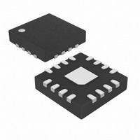
MAX6966ATE+ Maxim Integrated Products, MAX6966ATE+ Datasheet - Page 10

MAX6966ATE+
Manufacturer Part Number
MAX6966ATE+
Description
IC LED DRIVER LINEAR 16-TQFN
Manufacturer
Maxim Integrated Products
Type
Linear (Serial Interface)r
Datasheet
1.MAX6966ATE.pdf
(29 pages)
Specifications of MAX6966ATE+
Constant Current
Yes
Topology
Open Drain, PWM
Number Of Outputs
10
Internal Driver
Yes
Type - Primary
Backlight
Type - Secondary
RGB, White LED
Frequency
270kHz ~ 450kHz
Voltage - Supply
2.25 V ~ 3.6 V
Voltage - Output
7V
Mounting Type
Surface Mount
Package / Case
16-TQFN Exposed Pad
Operating Temperature
-40°C ~ 125°C
Current - Output / Channel
20mA
Internal Switch(s)
Yes
Number Of Segments
10
Low Level Output Current
21100 uA
Operating Supply Voltage
2.25 V to 3.6 V
Maximum Supply Current
4 mA
Maximum Power Dissipation
1176 mW
Maximum Operating Temperature
+ 125 C
Mounting Style
SMD/SMT
Minimum Operating Temperature
- 40 C
Lead Free Status / RoHS Status
Lead free / RoHS Compliant
Efficiency
-
Lead Free Status / Rohs Status
Lead free / RoHS Compliant
10-Port Constant-Current LED Drivers and I/O
Expanders with PWM Intensity Control
The MAX6966/MAX6967 contain 16 internal registers,
addressed as 0x00–0x09, and 0x10–0x15, which con-
figure and control the peripheral
addresses, 0x0E and 0x0F, do not store data but return
the port input status when read. Four virtual addresses,
Table 2. Register Address Map
10
Port P0 output level or PWM
Port P1 output level or PWM
Port P2 output level or PWM
Port P3 output level or PWM
Port P4 output level or PWM
Port P5 output level or PWM
Port P6 output level or PWM
Port P7 output level or PWM
Port P8 output level or PWM
Port P9 output level or PWM
Write ports P0 through P9 with same output level or
PWM
Read port P0 output level or PWM
Write ports P0 through P3 with same output level or
PWM
Read port P0 output level or PWM
Write ports P4 through P7 with same output level or
PWM
Read port P4 output level or PWM
Write ports P8 or P9 with same output level or PWM
Read port P8 output level or PWM
Read ports P7 through P0 inputs
Read ports P9 and P8 inputs
Configuration
Ramp-down
Ramp-up
Output current ISET70
Output current ISET98
Global current
No-op
Factory reserved; do not write to this register
______________________________________________________________________________________
REGISTER
Register Structure
(Table
2). Two
D15
R/W
R/W
R/W
R/W
R/W
R/W
R/W
R/W
R/W
R/W
R/W
R/W
R/W
R/W
R/W
R/W
R/W
R/W
0
1
0
1
0
1
0
1
1
1
D14
0x0A–0x0D allow more than one register to be written
with the same data to simplify software. The no-op
address, 0x20, causes no action when written or read,
and is used as a dummy register when accessing one
MAX6966/MAX6967 out of multiple cascaded devices.
0
0
0
0
0
0
0
0
0
0
0
0
0
0
0
0
0
0
0
0
0
0
0
1
D13
0
0
0
0
0
0
0
0
0
0
0
0
0
0
0
0
0
0
0
0
0
0
1
1
COMMAND ADDRESS
D12
0
0
0
0
0
0
0
0
0
0
0
0
0
0
0
0
1
1
1
1
1
1
0
1
D11
0
0
0
0
0
0
0
0
1
1
1
1
1
1
1
1
0
0
0
0
0
0
0
1
D10
0
0
0
0
1
1
1
1
0
0
0
0
1
1
1
1
0
0
0
0
1
1
0
1
D9
0
0
1
1
0
0
1
1
0
0
1
1
0
0
1
1
0
0
1
1
0
0
0
0
D8
0
1
0
1
0
1
0
1
0
1
0
1
0
1
0
1
0
1
0
1
0
1
0
1
CODE
0x0A
0x0B
0x0C
0x0D
0x7D
0x00
0x01
0x02
0x03
0x04
0x05
0x06
0x07
0x08
0x09
0x0E
0x0F
0x10
0x11
0x12
0x13
0x14
0x15
0x20
HEX


