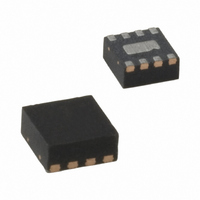
MIC2291-15YML TR Micrel Inc, MIC2291-15YML TR Datasheet - Page 7

MIC2291-15YML TR
Manufacturer Part Number
MIC2291-15YML TR
Description
IC LED DRIVER PHOTO FLASH 8-MLF
Manufacturer
Micrel Inc
Type
Photo Flash LEDr
Datasheet
1.MIC2291YD5_TR.pdf
(10 pages)
Specifications of MIC2291-15YML TR
Topology
PWM, Step-Up (Boost)
Number Of Outputs
1
Internal Driver
Yes
Type - Primary
Flash/Torch
Type - Secondary
White LED
Frequency
1.05MHz ~ 1.35MHz
Voltage - Supply
2.5 V ~ 10 V
Mounting Type
Surface Mount
Package / Case
8-MLF®, QFN
Operating Temperature
-40°C ~ 125°C
Current - Output / Channel
100mA
Internal Switch(s)
Yes
Lead Free Status / RoHS Status
Lead free / RoHS Compliant
Voltage - Output
-
Efficiency
-
Other names
576-1733-2
MIC2291-15YMLTR
MIC2291-15YMLTR
MIC2291-15YMLTR
MIC2291-15YMLTR
1-Cell
Application Information
DC to DC PWM Boost Conversion
The MIC2291 is a constant frequency boost converter. It
operates by taking a DC input voltage and regulating
cur-rent through series LED’s by monitoring voltage
across the sense resistor (R2). LED current regulation is
achieved by turning on an internal switch, which draws
current through the inductor (L1). When the switch turns
off, the inductor’s magnetic field collapses, causing the
current to be discharged into the output capacitor
through an external schottkey diode (D1). Regulation is
then achieved by pulse width modulation (PWM) to
maintain a constant voltage on the FB pin. This in turn
provides constant LED current.
Duty Cycle Considerations
Duty cycle refers to the switch on-to-off time ratio and
can be calculated as follows for a boost regulator;
The duty cycle required for voltage conversion should be
less than the maximum duty cycle of 85%. Also, in light
load conditions where the input voltage is close to the
output volt-age, the minimum duty cycle can cause pulse
skipping. This is due to the energy stored in the inductor
causing the output to overshoot slightly over the
regulated output voltage. During the next cycle, the error
amplifier detects the output as being high and skips the
following pulse. This effect can be reduced by increasing
the minimum load or by increasing the inductor value.
Increasing the inductor value reduces peak current,
which in turn reduces energy transfer in each cycle.
Li Ion
Micrel, Inc.
May 2007
GND
V
IN
Figure 2. DC to DC PWM Boost Conversion
D =
1
V
V
OUT
IN
MIC2291-34xML
VIN
EN
10µH
GND
OVP
SW
FB
Schottky
3xLED
1A/40V
D1
R2
V
GND
OUT
C2
1µF
7
Over Voltage Protection
For MLF
protection function. If the feedback resistors are
disconnected from the circuit or the feedback pin is
shorted to ground, the feedback pin will fall to ground
potential. This will cause the MIC2291 to switch at full
duty-cycle in an attempt to maintain the feedback
voltage. As a result the output voltage will climb out of
control. This may cause the switch node voltage to
exceed its maximum voltage rating, possibly damaging
the IC and the external components. To ensure the
highest level of protection, the MIC2291 OVP pin will
shut the switch off when an over-voltage condition is
detected saving itself and other sensitive circuitry
downstream.
Component Selection
Inductor
Inductor selection is a balance between efficiency,
stability, cost, size and rated current. For most
applications a 10µH is the recommended inductor value.
It
considerations.
Efficiency is affected by inductance value in that larger
inductance values reduce the peak to peak ripple
current. This has an effect of reducing both the DC
losses and the transition losses. There is also a
secondary effect of an inductors DC resistance (DCR).
The DCR of an inductor will be higher for more
inductance in the same package size. This is due to the
longer windings required for an increase in inductance.
Since the majority of input current (minus the MIC2291
operating current) is passed through the inductor, higher
DCR inductors will reduce efficiency.
Also, to maintain stability, increasing inductor size will
have to be met with an increase in output capacitance.
This is due to the unavoidable “right half plane zero”
effect for the continuous current boost converter
topology. The frequency at which the right half plane
zero occurs can be calculated as follows;
The right half plane zero has the undesirable effect of
increasing gain, while decreasing phase. This requires
that the loop gain is rolled off before this has significant
effect on the total loop response. This can be
accomplished by either reducing inductance (increasing
RHPZ frequency) or increasing the output capacitor
value (decreasing loop gain).
is
usually
®
frhpz
package of MIC2291, there is an over voltage
=
V
a
OUT
good
×
L
V
×
IN
I
2
OUT
balance
×
2
π
between
M9999-051507
MIC2291
these


