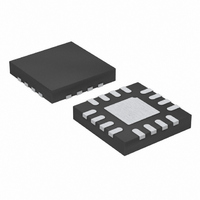
LTC3210EPD-1#TRPBF Linear Technology, LTC3210EPD-1#TRPBF Datasheet - Page 13

LTC3210EPD-1#TRPBF
Manufacturer Part Number
LTC3210EPD-1#TRPBF
Description
IC LED DRVR WHITE BCKLT 16-UTQFN
Manufacturer
Linear Technology
Type
Backlight, White LEDr
Datasheet
1.LTC3210EUD-1PBF.pdf
(16 pages)
Specifications of LTC3210EPD-1#TRPBF
Topology
Step-Up (Boost), Switched Capacitor (Charge Pump)
Number Of Outputs
5
Internal Driver
Yes
Type - Primary
Backlight
Type - Secondary
White LED
Frequency
800kHz
Voltage - Supply
2.9 V ~ 4.5 V
Mounting Type
Surface Mount
Package / Case
16-UTQFN (16-µTQFN)
Operating Temperature
-40°C ~ 85°C
Internal Switch(s)
Yes
Lead Free Status / RoHS Status
Lead free / RoHS Compliant
Voltage - Output
-
Current - Output / Channel
-
Efficiency
-
Available stocks
Company
Part Number
Manufacturer
Quantity
Price
applicaTions inFormaTion
• The flying capacitors must be placed close to the part.
• V
• LED pads must be large and connected to other layers
• RM and RC pins are sensitive to noise and capacitance.
Power Efficiency
To calculate the power efficiency (η) of a white LED
driver chip, the LED power should be compared to the
input power. The difference between these two numbers
represents lost power whether it is in the charge pump
or the current sources. Stated mathematically, the power
efficiency is given by:
The efficiency of the LTC3210-1 depends upon the mode in
which it is operating. Recall that the LTC3210-1 operates
as a pass switch, connecting V
is detected at the LED pin. This feature provides the op-
timum efficiency available for a given input voltage and
LED forward voltage. When it is operating as a switch, the
efficiency is approximated by:
since the input current will be very close to the sum of
the LED currents.
The traces from the pins to the capacitor pad should
be as wide as possible.
and handle high currents.
of metal to ensure proper heat sinking.
The resistors should be placed near the part with mini-
mum line width.
η =
η =
BAT
, CPO traces must be wide to minimize inductance
P
P
P
P
LED
LED
IN
IN
=
(
(
V
V
LED LED
BAT
•
•
I
I
BAT
)
)
=
V
V
BAT
LED
BAT
to CPO, until dropout
At moderate to high output power, the quiescent current
of the LTC3210-1 is negligible and the expression above
is valid.
Once dropout is detected at any LED pin, the LTC3210-1
enables the charge pump in 1.5x mode.
In 1.5x boost mode, the efficiency is similar to that of a
linear regulator with an effective input voltage of 1.5 times
the actual input voltage. This is because the input current
for a 1.5x charge pump is approximately 1.5 times the
load current. In an ideal 1.5x charge pump, the power
efficiency would be given by:
Similarly, in 2x boost mode, the efficiency is similar to
that of a linear regulator with an effective input voltage
of 2 times the actual input voltage. In an ideal 2x charge
pump, the power efficiency would be given by:
Thermal Management
For higher input voltages and maximum output current,
there can be substantial power dissipation in the LTC3210-1.
If the junction temperature increases above approximately
150°C the thermal shut down circuitry will automatically
deactivate the output current sources and charge pump.
To reduce maximum junction temperature, a good thermal
connection to the PC board is recommended. Connecting
the exposed pad to a ground plane and maintaining a solid
ground plane under the device will reduce the thermal
resistance of the package and PC board considerably.
η
η
IDEAL
IDEAL
=
=
P
P
P
P
LED
LED
IN
IN
=
=
(
(
V
V
(
BAT
BAT
V
(
V
LED LED
LED LED
•( ) •
•( . ) •
2
•
1 5
I
•
I
I
LED
)
I
LED
)
LTC3210-1
)
=
)
( •
= =
2
( . •
V
1 5
L L ED
V
BAT
V
LED
V
)
BAT
32101fd
)


