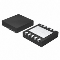
LTC3454EDD#TRPBF Linear Technology, LTC3454EDD#TRPBF Datasheet - Page 7

LTC3454EDD#TRPBF
Manufacturer Part Number
LTC3454EDD#TRPBF
Description
IC LED DRIVER PHOTO FLASH 10-DFN
Manufacturer
Linear Technology
Type
Photo Flash LEDr
Datasheet
1.LTC3454EDDPBF.pdf
(12 pages)
Specifications of LTC3454EDD#TRPBF
Topology
PWM, Step-Down (Buck), Step-Up (Boost)
Number Of Outputs
1
Internal Driver
Yes
Type - Primary
Backlight, Flash/Torch
Type - Secondary
White LED
Frequency
900MHz ~ 1.15MHz
Voltage - Supply
2.7 V ~ 5.5 V
Voltage - Output
5.15V
Mounting Type
Surface Mount
Package / Case
10-DFN
Operating Temperature
-40°C ~ 85°C
Current - Output / Channel
1A
Internal Switch(s)
Yes
Efficiency
90%
Lead Free Status / RoHS Status
Lead free / RoHS Compliant
Available stocks
Company
Part Number
Manufacturer
Quantity
Price
OPERATION
Buck-Boost DC/DC Converter
The LTC3454 employs an LTC proprietary buck-boost
DC/DC converter to generate the output voltage required to
drive a high current LED. This architecture permits high-
effi ciency, low noise operation at input voltages above,
below or equal to the output voltage by properly phasing
four internal power switches. The error amp output voltage
on the V
Since the V
of frequencies well below the factory trimmed switching
frequency of 1MHz. The low R
synchronous switches provide high frequency pulse width
modulation control at high effi ciency. Schottky diodes
across synchronous rectifi er switch B and synchronous
rectifi er switch D are not required, but if used do provide
a lower voltage drop during the break-before-make time
(typically 20ns), which improves peak effi ciency by typi-
cally 1% to 2% at higher loads.
Figure 1 shows a simplifi ed diagram of how the four internal
power switches are connected to the inductor, V
and GND. Figure 2 shows the regions of operation of the
buck-boost as a function of the control voltage V
output switches are properly phased so transitions between
regions of operation are continuous, fi ltered and transpar-
ent to the user. When V
region is reached where the conduction time of the four
switch region is typically 150ns. Referring to Figures 1
and 2, the various regions of operation encountered as V
increases will now be described.
Buck Mode (V
In buck mode, switch D is always on and switch C is
always off. Referring to Figure 2, when the control
voltage V
Figure 1. Simplifi ed Diagram of Internal Power Switches
C
C
pin determines the duty cycle of the switches.
is above voltage V1, switch A begins to turn on
V
C
9
IN
pin is a fi ltered signal, it provides rejection
PMOS A
NMOS B
IN
> V
SW1
10
OUT
IN
)
approaches V
SW2
6
DS(ON)
V
OUT
7
OUT
, low gate charge
3454 F01
PMOS D
NMOS C
, the buck-boost
IN
, V
C
. The
OUT
C
each cycle. During the off time of switch A, synchronous
rectifi er switch B turns on for the remainder of the cycle.
Switches A and B will alternate conducting similar to a
typical synchronous buck regulator. As the control volt-
age increases, the duty cycle of switch A increases until
the maximum duty cycle of the converter in buck mode
reaches DC
where DC
switch” range.
where f is the operating frequency in Hz.
Beyond this point the “four switch” or buck-boost region
is reached.
Buck-Boost or 4-Switch Mode (V
Referring to Figure 2, when the control voltage V
voltage V2, switch pair AD continue to operate for duty
cycle DC
in. As switch pair AC phases in, switch pair BD phases out
accordingly. When the V
buck-boost range at voltage V3, switch pair AC completely
phases out switch pair BD and the boost region begins at
duty cycle DC
switch region begins is given by:
and the input voltage V
ends is given by
BOOST
BOOST
DC
DC
V
V
CYCLE
D
D
BUCK
DUTY
D
IN
IN
75%
MAX
MAX
MIN
0%
BUCK
4SW
= V
= V
Figure 2. Switch Control vs Control Voltage, V
BUCK
FOUR SWITCH PWM
PWM CD SWITCHES
PWM AB SWITCHES BUCK REGION
OUT
OUT
= (150ns • f) • 100%
4SW
|Max = 100% – DC
BUCK
A ON, B OFF
D ON, C OFF
|max, and the switch pair AC begins to phase
/[1 – (150ns • f)]
• (1 – DC
4SW
equals the duty cycle in % of the “four
|Max given by:
. The input voltage V
BOOST REGION
4SW
IN
C
voltage reaches the edge of the
where the four switch region
) = V
BUCK/BOOST REGION
4SW
OUT
IN
≈ V
• [1 – (150ns • f)]
IN
LTC3454
OUT
3454 F02
where the four
)
V4 (2.1V)
V3 (1.65V)
V2 (1.55V)
V1 (0.9V)
CONTROL
VOLTAGE, V
C
C
is above
3454fa
C
7


