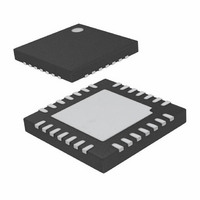
LTC3220IPF#PBF Linear Technology, LTC3220IPF#PBF Datasheet - Page 7

LTC3220IPF#PBF
Manufacturer Part Number
LTC3220IPF#PBF
Description
IC LED DRVR QVGA DISPLAY 28UTQFN
Manufacturer
Linear Technology
Type
QVGA Display (I²C Interface)r
Datasheet
1.LTC3220EPFPBF.pdf
(20 pages)
Specifications of LTC3220IPF#PBF
Topology
Open Drain, Step-Up (Boost), Switched Capacitor (Charge Pump)
Number Of Outputs
18
Internal Driver
Yes
Type - Primary
Backlight
Type - Secondary
LED Blinker
Frequency
850kHz ~ 1.05MHz
Voltage - Supply
2.9 V ~ 5.5 V
Mounting Type
Surface Mount
Package / Case
28-UTQFN
Operating Temperature
-40°C ~ 125°C
Current - Output / Channel
20mA
Internal Switch(s)
Yes
Efficiency
91%
Operating Supply Voltage (typ)
3.3/5V
Number Of Segments
18
Operating Temperature (min)
-40C
Operating Temperature (max)
125C
Operating Temperature Classification
Automotive
Package Type
UTQFN EP
Pin Count
28
Mounting
Surface Mount
Operating Supply Voltage (min)
2.9V
Operating Supply Voltage (max)
5.5V
Lead Free Status / RoHS Status
Lead free / RoHS Compliant
Voltage - Output
-
Lead Free Status / Rohs Status
Compliant
Available stocks
Company
Part Number
Manufacturer
Quantity
Price
PIN FUNCTIONS
SDA (Pin 12): Input Data for the Serial Port. Serial data is
shifted in one bit per clock cycle to control the LTC3220/
LTC3220-1. The logic level is referenced to DV
C1P , C2P , C1M, C2M (Pins 27, 26, 23, 22): Charge Pump
Flying Capacitor Pins. A 2.2μF X7R or X5R ceramic ca-
pacitor should be connected from C1P to C1M and C2P
to C2M.
V
must be bypassed with a single 2.2μF low ESR ceramic
capacitor.
BLOCK DIAGRAM
IN
(Pin 24): Supply Voltage for the Entire Device. This pin
24
10
25
12
11
V
DV
RST
SDA
SCL
IN
CC
21
ULED18
20
ULED17
+
–
19
ULED16
CC
1.22V
SHIFT REGISTER
MASTER/SLAVE
OSCILLATOR
18
.
CONTROL
ULED15
850kHz
LOGIC
REG
17
ULED14
RST (Pin 25): Active Low Reset Input. RST Resets all
internal registers and forces LTC3220/LTC3220-1 into
shutdown mode.
CPO (Pin 28): Output of the Charge Pump. Used to power
all LEDs. A 4.7μF X5R or X7R ceramic capacitor should
be connected to ground.
Exposed Pad (Pin 29): Ground. The Exposed Pad must
be soldered to PCB ground.
16
ULED13
27
C1P
15
ULED12
CHARGE PUMP
23
CURRENT SOURCES
C1M
18 UNIVERSAL
AND DACS
14
ULED11
26
LTC3220/LTC3220-1
C2P
13
22
ULED10
C2M
18
9
ULED9
EXPOSED
ULED1
ULED2
ULED3
ULED4
ULED5
ULED6
ULED7
ULED8
PAD
CPO
3220 BD
29
28
1
2
3
4
5
6
7
8
32201fc
7


