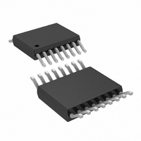
LT3519IMS-1#TRPBF Linear Technology, LT3519IMS-1#TRPBF Datasheet - Page 8

LT3519IMS-1#TRPBF
Manufacturer Part Number
LT3519IMS-1#TRPBF
Description
LED DRIVER WITH INTEGRATED SCHOT
Manufacturer
Linear Technology
Type
High Power, Constant Currentr
Datasheet
1.LT3519EMS-2PBF.pdf
(20 pages)
Specifications of LT3519IMS-1#TRPBF
Constant Current
Yes
Constant Voltage
Yes
Topology
PWM, SEPIC, Step-Down (Buck), Step-Up (Boost)
Number Of Outputs
1
Internal Driver
Yes
Type - Primary
Automotive
Frequency
800kHz ~ 1.10MHz
Voltage - Supply
3 V ~ 30 V
Mounting Type
Surface Mount
Package / Case
16-MSOP
Operating Temperature
-40°C ~ 125°C
Current - Output / Channel
750mA
Internal Switch(s)
Yes
Lead Free Status / RoHS Status
Lead free / RoHS Compliant
Voltage - Output
-
Efficiency
-
Available stocks
Company
Part Number
Manufacturer
Quantity
Price
OPERATION
LT3519/LT3519-1/LT3519-2
The LT3519/LT3519-1/LT3519-2 are constant frequency,
current mode regulators with an internal power switch and
Schottky. Operation can be best understood by referring
to the Block Diagram. At the start of each oscillator cycle,
the SR latch is set, which turns on the Q1 power switch.
A voltage proportional to the switch current is added to
a stabilizing ramp and the resulting sum is fed into the
positive terminal of the PWM comparator, A4. When this
voltage exceeds the level at the negative input of A4, the
SR latch is reset, turning off the power switch. The level
at the negative input of A4 is set by the error amplifi er A3.
A3 has two inputs, one from the voltage feedback loop and
the other one from the current loop. Whichever feedback
input is lower takes precedence to set the V
and forces the converter into either a constant-current or
a constant-voltage mode.
The LT3519/LT3519-1/LT3519-2 are designed to transi-
tion cleanly between these two modes of operation. The
current sense amplifi er senses the voltage across R
and provides an ×4 pre-gain to amplifi er A1. The output
of A1 is simply an amplifi ed version of the difference be-
tween the voltage across R
or 1.1V. In this manner, the error amplifi er sets the correct
peak switch current level to regulate the current through
R
current is delivered to the output; if it decreases, less
current is delivered. The current regulated in R
be adjusted by changing the input voltage V
voltage loop is implemented by the amplifi er A2. When
the voltage loop dominates, the V
the amplifi ed difference of the internal reference of 1.22V
and the FB pin. If FB voltage is lower than the reference
8
SENSE
. If the error amplifi er’s output increases, more
SENSE
C
and the lower of V
node voltage is set by
C
node voltage,
CTRL
SENSE
. The FB
SENSE
CTRL
can
voltage, the switch current will increase; if FB voltage is
higher than the reference voltage, the switch demand
current will decrease. The LED current sense feedback
interacts with the FB voltage feedback so that FB will not
exceed the internal reference and the voltage between ISP
and ISN will not exceed the threshold set by the CTRL pin.
For accurate current or voltage regulation, it is necessary
to be sure that under normal operating conditions the
appropriate loop is dominant. To deactivate the voltage
loop entirely, FB can be connected to GND. To deactivate
the LED current loop entirely, the ISP and ISN should be
tied together and the CTRL input tied to V
When the FB input exceeds a voltage about 60mV lower
than the FB regulation voltage, the pull-down driver on
the OPENLED pin is activated. This function provides a
status indicator that the load may be disconnected and
the constant-voltage feedback loop is taking control of
the switching regulator.
Dimming of the LED array is accomplished by pulsing the
current using the PWM pin. When the PWM pin is low,
switching is disabled and the error amplifi er is turned off
so that it does not drive the V
on the V
the V
capacitor. This feature reduces transient recovery time.
When the PWM input again transitions high, the demand
current for the switch returns to the value just before PWM
last transitioned low. To further reduce transient recovery
time, an external MOSFET should be used to disconnect
the LED array current loop when PWM is low, stopping
C
OUT
C
from discharging.
node will be saved on the internal compensation
C
node are disabled so that the charge state of
C
node. Also, all internal loads
REF
.
3519fa


