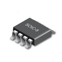
CY8CLEDAC02 Cypress Semiconductor Corp, CY8CLEDAC02 Datasheet - Page 11

CY8CLEDAC02
Manufacturer Part Number
CY8CLEDAC02
Description
IC CTLR AC-DC DIMMABLE LED 8SOIC
Manufacturer
Cypress Semiconductor Corp
Type
High Power, AC Input, Dimmabler
Datasheet
1.CY8CLEDAC02.pdf
(20 pages)
Specifications of CY8CLEDAC02
Package / Case
8-SOIC (3.9mm Width)
Voltage - Supply
8 V ~ 16 V
Frequency
200kHz
Operating Temperature
-40°C ~ 85°C
Number Of Outputs
1
Internal Switch(s)
No
Efficiency
85%
Topology
AC DC Offline Switcher
Operating Supply Voltage
- 0.3 V to 18 V
Maximum Supply Current
20 mA
Maximum Power Dissipation
526 mW
Maximum Operating Temperature
+ 85 C
Mounting Style
SMD/SMT
Minimum Operating Temperature
- 40 C
Operating Temperature (min)
-40C
Operating Temperature (max)
85C
Operating Temperature Classification
Industrial
Pin Count
8
Mounting
Surface Mount
Operating Supply Voltage (max)
18V
Lead Free Status / RoHS Status
Lead free / RoHS Compliant
Voltage - Output
-
Current - Output / Channel
-
Lead Free Status / Rohs Status
Lead free / RoHS Compliant
Available stocks
Company
Part Number
Manufacturer
Quantity
Price
Company:
Part Number:
CY8CLEDAC02
Manufacturer:
TI
Quantity:
900
Part Number:
CY8CLEDAC02
Manufacturer:
CYPRESS/赛普拉斯
Quantity:
20 000
Figure 12. Auxiliary Voltage Waveforms
The voltage at the load differs from the secondary voltage by a
diode drop and IR losses. The diode drop is a function of current,
as are IR losses. Thus, if the secondary voltage is always read
at a constant secondary current, the difference between the
output voltage and the secondary voltage is a fixed
if the voltage can be read when the secondary current is small;
for example, at the knee of the auxiliary waveform (see
Figure
can be ignored.
The real time waveform analyzer in the CY8CLEDAC02 reads
the auxiliary waveform information cycle by cycle. The part then
generates a feedback voltage V
represents the output voltage and is used to sense the output
voltage.
Document Number: 001-54879 Rev. *C
12), then
V is also small. With the CY8CLEDAC02,
FB_C
. The V
FB_C
signal precisely
V. Further,
V
Valley Mode Switching
To reduce EMI and switching losses in the MOSFET, the
CY8CLEDAC02 employs valley mode switching by switching at
the lowest MOSFET V
MOSFET drain voltage indirectly through the V
voltage is provided by the auxiliary winding of the flyback trans-
former and represents a copy of the secondary side character-
istics (see
Figure 13. Valley Mode Switching
Turning on at the lowest V
mode switching can also reduce EMI. To limit the switching
frequency range, the CY8CLEDAC02 can skip valleys (as shown
in the first cycle in
becomes too high.
Figure
12).
Figure
DS
(see
DS
13) when the switching frequency
generates lowest dV/dt; thus valley
Figure
13). It detects valleys in the
CY8CLEDAC02
SENSE
Page 11 of 20
pin. This
[+] Feedback


