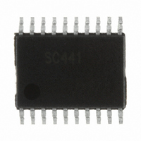
SC441TETRT Semtech, SC441TETRT Datasheet - Page 12

SC441TETRT
Manufacturer Part Number
SC441TETRT
Description
IC LED DRIVR WHT BCKLGT 20-TSSOP
Manufacturer
Semtech
Type
Backlight, White LEDr
Datasheet
1.SC441TETRT.pdf
(19 pages)
Specifications of SC441TETRT
Constant Current
Yes
Topology
PWM, Step-Up (Boost)
Number Of Outputs
4
Internal Driver
Yes
Type - Primary
Backlight
Frequency
560kHz ~ 840kHz
Voltage - Supply
4.5 V ~ 21 V
Voltage - Output
36V
Mounting Type
Surface Mount
Package / Case
20-TSSOP
Current - Output / Channel
150mA
Internal Switch(s)
Yes
Efficiency
90%
Lead Free Status / RoHS Status
Lead free / RoHS Compliant
Operating Temperature
-
Other names
SC441TETR
Applications Information (continued)
Referring to the Block Diagram, Figure 1, the clock from the
oscillation section resets the latch and turns on the power
transistor. Switch current is sensed with an integrated
sense resistor. The sensed current is summed with the
slope-compensating ramp and fed into the modulating
ramp input of the PWM comparator. The latch is set and
the power transistor conduction is terminated when
the modulating ramp intersects with the error amplifier
output (COMP).
The current-mode switching regulator is a dual-loop
feedback control system. In the inner current loop, the
EA output (COMP) controls the peak inductor current. In
the outer loop, the error amplifier regulates the output
voltage to keep the LED current at setting point. The
double reactive poles of the output LC filter are reduced
to a single real pole by the inner current loop, allowing
the simple loop compensation network to accommodate
a wide range of input and output voltages.
It is well known that, in Boost converter, Vo is greater than
or equal to Vin. In normal continuous conduction mode
(CCM) operation,
Where, D is the duty ratio of the PWM power switch. As
Vin increases, in order to regulate Vo to a given constant
value, D decreases. When Vin approaches Vo, D surely
leads to 0. In practice, due to the minimum on-time of
the PWM power switch, D usually could not approach 0
with infinitely small granularity. At some point, it either
produces one pulse with minimum on-time or generates
0 by skipping the pulse. Such point could be theoretically
calculated for SC441 as follows.
For CCM: Vin ≥ 0.92 Vo.
For DCM (Discontinuous conduction mode):
Where, Ro is the Boost equivalent output resistance (=Vo/
Io), L is the Boost inductor (in uH).
In many Boost converter designs and operations, pulse
skipping is normally allowed at light load conditions.
Some designers even purposely let the Boost power con-
verter enter the pulse skipping in order to save power at
light load conditions. If some designers do not want pulse
skipping mode, based on the conditions provided above,
© 2010 Semtech Corporation
V
in
≥
1
+
NOT RECOMMENDED FOR NEW DESIGNS: SEE SC441A
V
V
1
in
o
+
=
. 1
1
* 6
2
−
1
D
10
2 −
*
R
L
o
V
o
there are some choices.
1) Leave some room between Vin range and Vo.
2) Operate the Boost converter at normal load (less Ro)
3) Increases the Boost inductance (L).
Over-Current Protection
SC441 provides cycle-by-cycle current limiting for its
internal switch. If the switch current exceeds 3.32A (the
typical current-limit trip point), then the current-limit
comparator ILIM, will set the latch immediately turning off
internal power. All LED current sources keep operating in
an over-current condition. Due to separate pulse-width
modulating and current limiting paths, the OCP trip point
is not affected by slope compensation (i.e. trip point is not
affected by switching duty cycle).
Over-Voltage Protection (OVP)
SC441 includes an external programming over-voltage
protection circuit to prevent damage to the IC and output
capacitor in the event of an open-circuit condition. The
boost converter’s output voltage is detected at the OVPIN
pin. If the voltage at the OVPIN pin exceeds 1.55V (typical),
the boost converter will shut down and a 0.9mA pull-down
current will be applied to the VOUT pin to quickly discharge
the output capacitor. This added protection prevents a
condition where the output capacitor and Schottky diode
must endure high voltage for an extended time, which
can pose a reliability risk for the user’s system.
Refer to evaluation application circuit in page15. The
output over voltage trip point can be programmed by R5
and R7 resistor divider.
The relationship can be described as follows:
Where OVPIN_TH is 1.55V typical.
An OVP event causing a fault could disable the boost
converter enabling the device to a strong pull-down. This
event would cause the FFLAG pin to go high and the soft-
start capacitor to discharge. When the soft-start capacitor
voltage falls below 0.5V, and the output voltage falls to
VIN, SC441 enters a soft-start process.
The OVP detection circuitry provides a disconnect function
during the shutdown state to prevent any leakage from
the output. The external OVP resistor divider should be
connected between VOUT and OVPRTN with the central
OVP
_
trip
=
OVPIN
_
TH
×
R
5
R
www.semtech.com
+
7
R
7
SC441
12


