LM2753SDX/NOPB National Semiconductor, LM2753SDX/NOPB Datasheet - Page 4
LM2753SDX/NOPB
Manufacturer Part Number
LM2753SDX/NOPB
Description
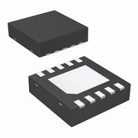
IC LED DRIVER PHOTO FLASH 10-LLP
Manufacturer
National Semiconductor
Type
Photo Flash LEDr
Datasheet
1.LM2753SDNOPB.pdf
(12 pages)
Specifications of LM2753SDX/NOPB
Topology
PWM, Switched Capacitor (Charge Pump)
Number Of Outputs
1
Internal Driver
Yes
Type - Primary
Flash/Torch
Type - Secondary
White LED
Frequency
725kHz
Voltage - Supply
3 V ~ 5.5 V
Voltage - Output
5V
Mounting Type
Surface Mount
Package / Case
10-LLP
Operating Temperature
-40°C ~ 85°C
Current - Output / Channel
250mA
Internal Switch(s)
Yes
Lead Free Status / RoHS Status
Lead free / RoHS Compliant
Efficiency
-
Other names
LM2753SDX
Available stocks
Company
Part Number
Manufacturer
Quantity
Price
Company:

Part Number:
LM2753SDX/NOPB
Manufacturer:
MAXIM
Quantity:
451


www.national.com
Note 5: In applications where high power dissipation and/or poor package thermal resistance is present, the maximum ambient temperature may have to be
derated. Maximum ambient temperature (T
dissipation of the device in the application (P
following equation: T
Note 6: Junction-to-ambient thermal resistance (θ
JEDEC standard JESD51-7. The test board is a 4 layer FR-4 board measuring 102mm x 76mm x 1.6mm with a 2 x 1 array of thermal vias. The ground plane on
the board is 50mm x 50mm. Thickness of copper layers are 36µm/18µm /18µm/36µm (1.5oz/1oz/1oz/1.5oz). Ambient temperature in simulation is 22°C, still air.
Power dissipation is 1W.
The value of θ
conditions. In applications where high maximum power dissipation exists (high V
information on these topics, please refer to Application Note 1187: Leadless Leadframe Package (LLP) and the Power Efficiency and Power Dissipation
section of this datasheet.
Note 7: Min and Max limits are guaranteed by design, test, or statistical analysis. Typical numbers are not guaranteed, but represent the most likely norm.
Note 8: C
Note 9: Turn-on time is measured from when the EN signal is pulled high until the output voltage on V
Note 10: Flash Turn-on time is measured from when the FLASH signal is pulled high until the voltage on I
Block Diagram
IN
, C
JA
OUT
of the LM2753 in LLP-10 could fall in a range as wide as 50ºC/W to 150ºC/W (if not wider), depending on PWB material, layout, and environmental
, and C
A-MAX
1
: Low-ESR Surface-Mount Ceramic Capacitors (MLCCs) used in setting electrical characteristics.
= T
J-MAX-OP
- (θ
JA
A-MAX
× P
D-MAX
D-MAX
) is dependent on the maximum operating junction temperature (T
), and the junction-to ambient thermal resistance of the part/package in the application (θ
JA
) is taken from a thermal modeling result, performed under the conditions and guidelines set forth in the
).
4
IN
, high I
OUT
), special care must be paid to thermal dissipation issues. For more
OUT
OUT
crosses 90% of its final value.
crosses 90% of its final programmed value.
J-MAX-OP
= 120ºC), the maximum power
20140606
JA
), as given by the
Related parts for LM2753SDX/NOPB
Image
Part Number
Description
Manufacturer
Datasheet
Request
R

Part Number:
Description:
IC,Laser Diode/LED Driver,LLCC,10PIN,PLASTIC
Manufacturer:
National Semiconductor

Part Number:
Description:
IC LED DRIVER PHOTO FLASH 10-LLP
Manufacturer:
National Semiconductor
Datasheet:
Part Number:
Description:
IC,Laser Diode/LED Driver,LLCC,10PIN,PLASTIC
Manufacturer:
National Semiconductor
Part Number:
Description:
National Semiconductor [8-Bit D/A Converter]
Manufacturer:
National Semiconductor
Datasheet:
Part Number:
Description:
National Semiconductor [Media Coprocessor]
Manufacturer:
National Semiconductor
Datasheet:
Part Number:
Description:
Digitally Controlled Tone and Volume Circuit with Stereo Audio Power Amplifier, Microphone Preamp Stage and National 3D Sound
Manufacturer:
National Semiconductor
Datasheet:
Part Number:
Description:
Digitally Controlled Tone and Volume Circuit with Stereo Audio Power Amplifier, Microphone Preamp Stage and National 3D Sound
Manufacturer:
National Semiconductor
Datasheet:
Part Number:
Description:
AC97 Rev 2 Codec with Sample Rate Conversion and National 3D Sound
Manufacturer:
National Semiconductor
Part Number:
Description:
Manufacturer:
National Semiconductor
Datasheet:
Part Number:
Description:
Manufacturer:
National Semiconductor
Datasheet:
Part Number:
Description:
General Purpose, Low Voltage, Low Power, Rail-to-Rail Output Operational Amplifiers
Manufacturer:
National Semiconductor
Datasheet:
Part Number:
Description:
8-bit 20 MSPS flash A/D converter.
Manufacturer:
National Semiconductor
Datasheet:
Part Number:
Description:
Low Noise Quad Operational Amplifier
Manufacturer:
National Semiconductor
Datasheet:
Part Number:
Description:
Quad Differential Line Receivers
Manufacturer:
National Semiconductor
Datasheet: