LM3503ITL-25/NOPB National Semiconductor, LM3503ITL-25/NOPB Datasheet
LM3503ITL-25/NOPB
Specifications of LM3503ITL-25/NOPB
LM3503ITL-25TR


Related parts for LM3503ITL-25/NOPB


LM3503ITL-25/NOPB Summary of contents
Page 1
... LED current control capability, the LM3503 offers superior performance over other step-up white LED drivers. Typical Application © 2006 National Semiconductor Corporation Features n Drives White LEDs for Dual Display Backlighting > ...
Page 2
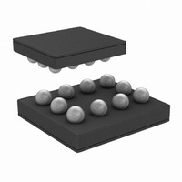
Connection Diagrams 10-Bump Thin MicroSMD Package (TLP10) Top View www.national.com 16-Lead Thin Leadless Leadframe Package (SQA16A) 20128602 2 20128603 Top View ...
Page 3
Pin Descriptions/Functions Bump # Pin # Name A1 9 Cntrl OUT2 OUT1 D2 2 and and 16 Pgnd C3 14 Agnd ...
Page 4
... LM3503ITLX-16 SBHB 16 LM3503SQ-16 L00045B 16 LM3503SQX-16 L00045B 25 LM3503ITL-25 SBJB 25 LM3503ITLX-25 SBJB 25 LM3503SQ-25 L00046B 25 LM3503SQX-25 L00046B 35 LM3503ITL-35 SBKB 35 LM3503ITLX-35 SBKB 35 LM3503SQ-35 L00047B 35 LM3503SQX-35 L00047B 44 LM3503ITL-44 SDNB 44 LM3503ITLX-44 SDNB 44 LM3503SQ-44 L00053B 44 LM3503SQX-44 L00053B www.national.com Package Marking 250 Units, Tape-and-Reel 3000 Units, Tape-and-Reel 1000 Units, Tape-and-Reel ...
Page 5
... Absolute Maximum Ratings If Military/Aerospace specified devices are required, please contact the National Semiconductor Sales Office/ Distributors for availability and specifications. V Pin IN Sw Pin Fb Pin Cntrl Pin V Pin OUT1 V Pin OUT2 En1 En2 Continuous Power Dissipation Maximum Junction Temperature (T ) J-MAX Storage Temperature Range Electrical Characteristics face apply over the full operating junction temperature range (− ...
Page 6
Electrical Characteristics typeface apply over the full operating junction temperature range (−40˚C ≤ T 2.5V. (Continued) Symbol Parameter I V Pin Leakage Fb = En1 = En2 = 0V OUT2 OUT2 Current (Note 3) UVP Under-Voltage On Threshold ...
Page 7
Block Diagram FIGURE 1. Block Diagram 7 20128604 www.national.com ...
Page 8
Detailed Description of Operation The LM3503 utilizes an asynchronous current mode pulse- width-modulation (PWM) control scheme to regulate the feedback voltage over specified load conditions. The DC/DC converter behaves as a controlled current source for white LED applications. The operation ...
Page 9
Typical Performance Characteristics D=B150-13. Efficiency: η [(V OUT IN I (Non-Switching (Switching LED Efficiency vs LED Current (See Typical Application Circuit : L=DO1608C-223 and – ...
Page 10
Typical Performance Characteristics D=B150-13. Efficiency: η OUT 6 LED Efficiency vs LED Current Cntrl Pin Current vs Cntrl Pin Voltage En1 Pin Current vs En1 Pin Voltage www.national.com (See Typical Application Circuit : L=DO1608C-223 and = ...
Page 11
Typical Performance Characteristics D=B150-13. Efficiency: η [(V OUT IN V Pin Current vs V OUT1 OUT1 NMOS R (Figure 1: N2 DS(ON) Feedback Voltage vs Cntrl Pin Voltage (See Typical Application Circuit : ...
Page 12
Typical Performance Characteristics D=B150-13. Efficiency: η OUT Current Limit (LM3503-16 Current Limit (LM3503-25 Current Limit (LM3503-35/44 www.national.com (See Typical Application Circuit : L=DO1608C-223 and = [(V – ...
Page 13
Typical Performance Characteristics D=B150-13. Efficiency: η [(V OUT IN Feedback Voltage (V = 1.6V) vs Temp Cntrl V = 3.6V at 15mA & 2 Leds IN (See Typical Application Circuit : L=DO1608C-223 and – V ...
Page 14
Application Information WHITE LED CURRENT SETTING The white LED current is controlled voltage at the Cntrl pin. The relationship between the Cntrl pin voltage and Fb pin voltage can be computed with the following: : Cntrl Pin ...
Page 15
Application Information PWM Dimming Duty Cycle vs. LED Current The results are based on the 2LEDs on Main display and 2LEDs on Sub display Duty 200Hz 500Hz (%) R = 787k ohms R =316k ohms 10 0.78mA 1.59mA 20 1.85mA ...
Page 16
Application Information V : Input Voltage Output Voltage. OUT Eff: Efficiency of the LM3503. Fs: Switching Frequency White LED Current/Load Current. OUT L: Inductance Magnitude/Inductor Value. D: Duty Cycle for CCM operation. ∆i : Inductor ...
Page 17
Application Information INPUT CAPACITOR SELECTION The input capacitor serves as an energy reservoir for the inductor. In addition to acting as an energy reservoir for the inductor the input capacitor is necessary for the reduction in input voltage ripple and ...
Page 18
Application Information capacitor can be placed in parallel with C frequency noise to ground. The output capacitor placed close to the IC and be connected between the V and Pgnd pins. Any copper trace connections for the OUT1 ...
Page 19
Physical Dimensions inches (millimeters) unless otherwise noted TLP10: 10-Bump Thin Micro SMD Package X1 = 1.958 2.135 0 Package Number TLP10 16-Lead Thin Leadless Leadframe Package NS Package Number SQA16A 19 www.national.com ...
Page 20
... BANNED SUBSTANCE COMPLIANCE National Semiconductor follows the provisions of the Product Stewardship Guide for Customers (CSP-9-111C2) and Banned Substances and Materials of Interest Specification (CSP-9-111S2) for regulatory environmental compliance. Details may be found at: www.national.com/quality/green. ...