NCP5623AMUTBG ON Semiconductor, NCP5623AMUTBG Datasheet
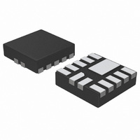
IC LED DRIVER RGB 12-LLGA

NCP5623AMUTBG

Manufacturer Part Number
NCP5623AMUTBG
Description
IC LED DRIVER RGB 12-LLGA
Manufacturer
ON Semiconductor
Type
RGB LED Driverr
Datasheet

Specifications of NCP5623AMUTBG

Topology
PWM, Switched Capacitor (Charge Pump)
Number Of Outputs
3
Internal Driver
Yes
Type - Primary
Backlight, Flash/Torch
Type - Secondary
RGB, White LED
Frequency
800kHz ~ 1.2kHz
Voltage - Supply
2.7 V ~ 5.5 V
Voltage - Output
4.4 V ~ 5.7 V
Mounting Type
Surface Mount
Package / Case
12-LLGA
Operating Temperature
-40°C ~ 85°C
Current - Output / Channel
90mA
Internal Switch(s)
Yes
Efficiency
94%
Lead Free Status / RoHS Status
Lead free / RoHS Compliant
NCP5623
Triple Output I2C Controlled
RGB LED Driver
dedicated to the RGB illumination or backlight LCD display.
Features
Typical Applications
© Semiconductor Components Industries, LLC, 2008
August, 2008 ï Rev. 6
I2C Port
The NCP5623 mixed analog circuit is a triple output LED driver
2.7 to 5.5 V Input Voltage Range
RGB Function Fully Supported
Programmable Integrated Gradual Dimming
90 mA Total LED Current Capability
Provides Three Independent LED Drives
Support I2C Protocol
This is a PbïFree Device
Multicolor Illuminations
Portable Back Light
Digital Cellular Phone Camera Photo Flash
LCD and Key Board Simultaneous Drive
+Vcc
MCU
Figure 1. Typical Multiple Color LED Driver
SDA
SCL
GND
1 mF/6.3 V
GND
GND
C1
62 k
+Vbat
R1
13
12
10
11
9
6
2
1
Vbat
Vdet
SDA
SCL
IREF
GND
GND
IC NC NC IC
NCP5623
7
U1
8 14
LED1
LED2
LED3
5
4
3
GND
6
2
5
LRTBïG6T
1 mF/6.3 V
D1
C2
R
G
B
1
1
3
4
+5 V
14
†For information on tape and reel specifications,
NCP5623DTBR2G
This document contains information on a
product under development. ON Semiconductor
reserves the right to change or discontinue this
product without notice.
This document, and the information contained herein,
is CONFIDENTIAL AND PROPRIETARY and the
property of Semiconductor Components Industries,
LLC., dba ON Semiconductor. It shall not be used,
published, disclosed or disseminated outside of the
Company, in whole or in part, without the written
permission
engineering of any or all of the information contained
herein is strictly prohibited.
including part orientation and tape sizes, please
refer to our Tape and Reel Packaging Specification
Brochure, BRD8011/D.
(Note: Microdot may be in either location)
Device
E 2008, SCILLC. All Rights Reserved.
ORDERING INFORMATION
5623
A
L
Y
W
G
1
of
http://onsemi.com
ON
= Specific Device Code
= Assembly Location
= Wafer Lot
= Year
= Work Week
= PbïFree Package
CASE 948G
TSSOPï14
TSSOPï14
(PbïFree)
Package
Semiconductor.
Publication Order Number:
14
1
MARKING
DIAGRAM
Tape & Reel
Shipping
NCP5623/D
ALYWG
2500 /
5623
Reverse
G

Related parts for NCP5623AMUTBG

NCP5623AMUTBG Summary of contents

Page 1

... This document, and the information contained herein, is CONFIDENTIAL AND PROPRIETARY and the property of Semiconductor Components Industries, LLC., dba ON Semiconductor. It shall not be used, published, disclosed or disseminated outside of the Company, in whole or in part, without the written permission of ON Semiconductor ...

Page 2

Vbat 1 mF/6 GND 6 GND DIGITAL CONTROL SDA 9 SCL 11 Vbat R1 ANALOG 10 FUNCTIONS 62 k GND NCP5623 TSSOPï GND 13 Vbat 2 Vdet LED3 SCL ...

Page 3

PIN ASSIGNMENT Pin Name Type 1 IC This pin is internally connected. It must be left open. 2 GND POWER This pin is the GROUND signal for the analog and digital blocks and output current control. The pin must be ...

Page 4

MAXIMUM RATINGS Symbol V Power Supply (see Figure 4) bat SDA, SCL Digital Input Voltage Human Body Model 1500 100 pF (Note 3) ESD Machine Model P Power Dissipation @ Thermal Resistance ...

Page 5

ANALOG SECTION: (Typical values are referenced +25°C, Min & Max values are referenced ï40°C to +85°C ambient temperature, unless otherwise A noted), operating conditions 2.85 V < V < 5.5 V, unless otherwise noted. bat Pin Symbol ...

Page 6

LED MAXIMUM CURRENT CALCULATION The load current is derived from the 600 mV reference voltage provided by the internal Band Gap associated to the external resistor connected across I REF Note : due to the internal structure of this pin, ...

Page 7

B[7:5] : Internal Register Selection The contain of bits B[4:0] depends upon the type of function selected by bits B[7:5] as ...

Page 8

Table 2. Basic Programming Sequences I2C Address COMMAND Bits[7:0] $70 000X XXXX $70 0010 0000 0011 1111 $70 0100 0000 0101 1111 $70 0110 0000 0111 1111 $70 1000 0000 1001 1111 $70 1010 0000 1011 1111 $70 1100 0000 ...

Page 9

Figure 5. Output Current Programmed Value ( ILED = F(Step) ) PWM OPERATION The builtïin PWM are fully independent and can be programmed to any value during the normal operation of the ...

Page 10

... PbïFree strategy and soldering details, please download the ON Semiconductor Soldering and Mounting Techniques Reference Manual, SOLDERRM/D. ON Semiconductor and are registered trademarks of Semiconductor Components Industries, LLC (SCILLC). SCILLC reserves the right to make changes without further notice to any products herein ...

Related keywords