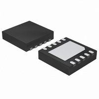
NCP5603MNR2G ON Semiconductor, NCP5603MNR2G Datasheet - Page 4

NCP5603MNR2G
Manufacturer Part Number
NCP5603MNR2G
Description
IC LED DRIVR WHITE BCKLGT 10-DFN
Manufacturer
ON Semiconductor
Type
Backlight, White LEDr
Datasheet
1.NCP5603MNR2G.pdf
(13 pages)
Specifications of NCP5603MNR2G
Constant Voltage
Yes
Topology
PWM, Switched Capacitor (Charge Pump)
Number Of Outputs
1
Internal Driver
Yes
Type - Primary
Backlight, Flash/Torch
Type - Secondary
White LED
Voltage - Supply
2.7 V ~ 5.5 V
Voltage - Output
4.75 V ~ 5.25 V
Mounting Type
Surface Mount
Package / Case
10-VFDFN Exposed Pad
Operating Temperature
-40°C ~ 85°C
Current - Output / Channel
200mA
Internal Switch(s)
Yes
Efficiency
90%
Number Of Segments
4
Operating Supply Voltage
2.85 V to 5.5 V
Maximum Supply Current
800 mA
Maximum Power Dissipation
580 mW
Maximum Operating Temperature
+ 85 C
Mounting Style
SMD/SMT
Minimum Operating Temperature
- 40 C
Lead Free Status / RoHS Status
Lead free / RoHS Compliant
Frequency
-
Lead Free Status / Rohs Status
Details
Other names
NCP5603MNR2G
NCP5603MNR2GOSTR
NCP5603MNR2GOSTR
Available stocks
Company
Part Number
Manufacturer
Quantity
Price
Company:
Part Number:
NCP5603MNR2G
Manufacturer:
FM
Quantity:
30 000
Part Number:
NCP5603MNR2G
Manufacturer:
ON/安森美
Quantity:
20 000
1. Using ceramic 16 V working voltage capacitors is recommended to compensate the DC bias effect encountered with such type of capacitors.
2. Any external impedance connected to pin 6 shall be 10 kW or higher.
PIN FUNCTION DESCRIPTION
Pin
10
1
2
3
4
5
6
7
8
9
EN/PWM
Symbol
GND
C1N
Vsel
C2N
C1P
C2P
V
Fsel
V
out
bat
OUTPUT, PWR
INPUT, Digital
INPUT, Digital
INPUT, Digital
GROUND
POWER
POWER
POWER
POWER
POWER
Type
This pin supplies the regulated voltage to the external LED. Since high current transients
are present in this pin, care must be observed to avoid voltage spikes in the system. Good
high frequency layout technique must be observed.
One side of the external charge pump capacitor (C
with C1P, pin 9. Using low ESR ceramic capacitor is recommended to optimize the Charge
Pump efficiency.
This pin shall be connected to the power source, and must be decoupled to Ground by a
low ESR capacitor (2.2 mF/6.3 V ceramic or better (see Note 1)).
This pin is used to program the operating frequency:
This pin setup the output voltage:
This pin controls the activity of the NCP5603 chip:
The NCP5603 can operate either in a continuous mode (EN/PWM = High), or can be
controlled by a PWM pulse applied to EN/PWM to dim the output light. When EN/PWM is
Low, the external load is disconnected from the converter, providing a very low standby
current. The pull down built-in resistance makes sure the chip is deactivated even if the
EN/PWM pin is disconnected (see Note 2).
One side of the external charge pump capacitor (C
with C2P, pin 10. Using low ESR ceramic capacitor is recommended to optimize the
Charge Pump efficiency.
This pin combines the Signal ground and the Power ground and must be connected to the
system ground. Using good quality ground plane is mandatory to avoid spikes on the logic
signal lines.
One side of the external charge pump capacitor (C
with C1N, pin 2. Using low ESR ceramic capacitor is recommended to optimize the Charge
Pump efficiency.
One side of the external charge pump capacitor is connected to this pin, associated with
C2N, pin 7. Using low ESR ceramic capacitor is recommended to optimize the Charge
Pump efficiency.
Fsel = 0 → Fop = 262 kHz
Fsel = 1 → Fop = 650 kHz
Vsel = 0 → V
Vsel = 1 → V
EN/PWM = Low → the chip is deactivated, the load is disconnected
EN/PWM = High → the chip is activated and the load is connected to the
http://onsemi.com
regulated output current.
out
out
NCP5603
= 4.5 V
= 5.0 V
4
Description
FLY
FLY
FLY
) is connected to this pin, associated
) is connected to this pin, associated
) is connected to this pin, associated


