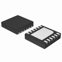
CAT3612HV2-GT2 ON Semiconductor, CAT3612HV2-GT2 Datasheet - Page 11

CAT3612HV2-GT2
Manufacturer Part Number
CAT3612HV2-GT2
Description
IC LED DVR CHRGE PUMP 2CH 12TDFN
Manufacturer
ON Semiconductor
Type
Photo Flash LEDr
Datasheet
1.CAT3612HV2-T2.pdf
(13 pages)
Specifications of CAT3612HV2-GT2
Topology
Linear (LDO), Switched Capacitor (Charge Pump)
Number Of Outputs
2
Internal Driver
Yes
Type - Primary
Flash/Torch
Frequency
800kHz ~ 1.3MHz
Voltage - Supply
3 V ~ 5.5 V
Voltage - Output
7V
Mounting Type
Surface Mount
Package / Case
12-VFDFN Exposed Pad
Operating Temperature
-40°C ~ 85°C
Current - Output / Channel
150mA
Internal Switch(s)
Yes
Efficiency
90%
Lead Free Status / RoHS Status
Lead free / RoHS Compliant
Available stocks
Company
Part Number
Manufacturer
Quantity
Price
Company:
Part Number:
CAT3612HV2-GT2
Manufacturer:
ON Semiconductor
Quantity:
1 400
Protection Mode
VOUT is internally limited to about 5.5 V. This is to prevent
the output pin from exceeding its absolute maximum rating.
die temperature exceeds about +165°C. When the device
temperature drops down by about 20°C, the device resumes
normal operation.
External Components
capacitors: two for decoupling input and output, and two for
the charge pump. Both capacitor types X5R and X7R are
recommended for the LED driver application. In the 1.5x
charge pump mode, the input current ripple is kept very low
by design, and an input bypass capacitor of 1 mF is sufficient.
In 1x mode, the device operating in linear mode does not
introduce switching noise back onto the supply.
If an LED becomes open−circuit, the output voltage
The driver enters a thermal shutdown mode as soon as the
The driver requires a total of four external 1 mF ceramic
http://onsemi.com
11
Recommended Layout
at a high frequency of 1 MHz. It is recommended to
minimize trace length to all four capacitors. A ground plane
should cover the area under the driver IC as well as the
bypass capacitors. Short connection to ground on capacitors
Cin and Cout can be implemented with the use of multiple
via. A copper area matching the TDFN exposed pad (GND)
must be connected to the ground plane underneath. The use
of multiple via improves the package heat dissipation.
In 1.5x charge pump mode, the driver switches internally
Figure 29. Recommended Layout


