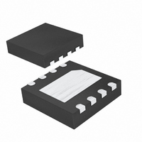
MAX8901BETA+T Maxim Integrated Products, MAX8901BETA+T Datasheet - Page 2

MAX8901BETA+T
Manufacturer Part Number
MAX8901BETA+T
Description
IC LED DRIVR WHITE BCKLGT 8-TDFN
Manufacturer
Maxim Integrated Products
Type
Backlight, White LEDr
Datasheet
1.MAX8901BETAT.pdf
(14 pages)
Specifications of MAX8901BETA+T
Constant Current
Yes
Topology
PWM, Step-Up (Boost)
Number Of Outputs
1
Internal Driver
Yes
Type - Primary
Backlight
Type - Secondary
White LED
Frequency
700kHz ~ 800kHz
Voltage - Supply
2.6 V ~ 5.5 V
Voltage - Output
24V
Mounting Type
Surface Mount
Package / Case
8-TDFN Exposed Pad
Operating Temperature
-40°C ~ 85°C
Current - Output / Channel
25mA
Internal Switch(s)
Yes
Efficiency
91%
Operating Supply Voltage
2.6 V to 5.5 V
Maximum Supply Current
185 uA
Maximum Power Dissipation
953 mW
Maximum Operating Temperature
+ 85 C
Mounting Style
SMD/SMT
Minimum Operating Temperature
- 40 C
Lead Free Status / RoHS Status
Lead free / RoHS Compliant
ABSOLUTE MAXIMUM RATINGS
IN to GND .................................................................-0.3V to +7V
CS, COMP, ON to GND ...............................-0.3V to (V
OVP, LX to GND .....................................................-0.3V to +28V
PGND to GND .......................................................-0.3V to +0.3V
LX Current ..................................................................770mA
Continuous Power Dissipation (multilayer board at +70°C)
Highest Efficiency Supply for 2 to 6
Series WLEDs in a 2mm x 2mm TDFN Package
Stresses beyond those listed under “Absolute Maximum Ratings” may cause permanent damage to the device. These are stress ratings only, and functional
operation of the device at these or any other conditions beyond those indicated in the operational sections of the specifications is not implied. Exposure to
absolute maximum rating conditions for extended periods may affect device reliability.
ELECTRICAL CHARACTERISTICS
(V
Typical values are at T
2
Input Voltage
Input Undervoltage Lockout
Threshold
Input Overvoltage Lockout
Threshold
Shutdown Input Current
Quiescent Current
Output Voltage Range
OVP Overvoltage Protection
Threshold
OVP Input Current
CS Regulation Voltage
ON Shutdown Delay
ON High Voltage
ON Low Voltage
ON Input Current
Initial ON High Pulse Width
ON High Pulse Width
ON Low Pulse Width
IN
8-pin, 2mm x 2mm TDFN
(derate above +70°C by 11.9mW/°C) ..........................953mW
_______________________________________________________________________________________
= V
ON
PARAMETER
= V
OVP
= 3.6V, V
A
= +25°C.) (Note 1)
PGND
= V
SYMBOL
V
V
V
GND
V
t
IN_UVLO
IN_OVLO
I
t
HI_INIT
V
SHDN
SHDN
ON_LO
ON_HI
V
V
I
V
I
t
OUT
t
ON
I
OV
LO
OV
HI
CS
Q
IN
= 0V, COMP, CS, and LX are unconnected, T
V
V
V
V
V
V
(not switching)
V
6 LEDs with 25V OVP option
V OVP = 20V
No dimming
Time V
shutdown (Figure 1)
2.6V < V
2.6V < V
ON = IN
First ON high pulse to enable IC
(MAX8901B) (Figure 1)
MAX8901B (Figure 1)
MAX8901B (Figure 1)
IN
IN
IN
IN
ON
CS
DIODE
IN
rising
falling
rising
falling
= 0.55V, no load
= 0V
+ 0.3V)
ON
= external boost diode voltage drop
IN
IN
RMS
is below low threshold until
< 5.5V
< 5.5V
CONDITIONS
Operating Temperature Range ...........................-40°C to +85°C
Junction Temperature ......................................................+150°C
Storage Temperature Range .............................-65°C to +150°C
Lead Temperature (soldering, 10s) .................................+300°C
Soldering Temperature (reflow) .......................................+260°C
T
T
MAX8901A
MAX8901B
T
T
A
A
A
A
= +25°C
= +85°C
= +25°C
= +85°C
A
= -40°C to +85°C, unless otherwise noted.
V
0.475
V
DIODE
2.25
1.18
MIN
2.6
6.2
6.0
1.3
0.5
0.5
24
40
IN
-
TYP
0.01
0.50
1.33
0.01
115
0.1
0.1
70
25
20
0.525
500.0
MAX
2.55
2.53
6.35
1.50
V
135
185
5.5
6.3
0.4
26
OV
1
1
UNITS
ms
µA
µA
µA
µA
µs
µs
µs
V
V
V
V
V
V
V
V


