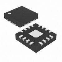
MAX6947ATE+T Maxim Integrated Products, MAX6947ATE+T Datasheet - Page 18

MAX6947ATE+T
Manufacturer Part Number
MAX6947ATE+T
Description
IC LED DRIVER LINEAR 16-TQFN
Manufacturer
Maxim Integrated Products
Type
Linear (I²C Interface)r
Datasheet
1.MAX6947ATE.pdf
(24 pages)
Specifications of MAX6947ATE+T
Constant Current
Yes
Topology
Open Drain, PWM
Number Of Outputs
10
Internal Driver
Yes
Type - Primary
Backlight
Type - Secondary
RGB, White LED
Frequency
400kHz
Voltage - Supply
2.25 V ~ 3.6 V
Voltage - Output
7V
Mounting Type
Surface Mount
Package / Case
16-TQFN Exposed Pad
Operating Temperature
-40°C ~ 125°C
Current - Output / Channel
20mA
Internal Switch(s)
Yes
Number Of Segments
3
Low Level Output Current
21.12 mA
Operating Supply Voltage
2.25 V to 3.6 V
Maximum Supply Current
60 uA
Maximum Power Dissipation
1176 mW
Maximum Operating Temperature
+ 125 C
Mounting Style
SMD/SMT
Minimum Operating Temperature
- 40 C
Lead Free Status / RoHS Status
Lead free / RoHS Compliant
Efficiency
-
Lead Free Status / Rohs Status
Details
If the MAX6946/MAX6947 operates on a 2-wire inter-
face with multiple masters, a master reading the
MAX6946/MAX6947 should use a repeated start
between the write. This sets the MAX6946/MAX6947
address pointer, and the read(s) that takes the data
from the location(s) (Table 1). This is because it is pos-
sible for master 2 to take over the bus after master 1
has set up the MAX6946/MAX6947s’ address pointer,
then master 1’s delayed read can be from an unexpect-
ed location.
The command address stored in the MAX6946/
MAX6947 increments through the grouped register func-
tions after each data byte is written or read (Table 1).
10-Port, Constant-Current LED Driver and
I/O Expander with PWM Intensity Control
Figure 12. Command Byte Received
Figure 13. Command and Single Data Byte Received
Figure 14. n Data Bytes Received
18
S
______________________________________________________________________________________
S
HOW COMMAND BYTE AND DATA BYTE MAP INTO
HOW COMMAND BYTE AND DATA BYTE MAP INTO
Command Address Autoincrementing
ACKNOWLEDGE FROM
ACKNOWLEDGE FROM
S
Operation with Multiple Masters
MAX6946/MAX6947s' REGISTERS
SLAVE ADDRESS
MAX6946/MAX6947s' REGISTERS
SLAVE ADDRESS
COMMAND BYTE IS STORED ON RECEIPT OF
MAX6946/MAX6947
MAX6946/MAX6947
ACKNOWLEDGE FROM MAX6946/MAX6947
SLAVE ADDRESS
R/W
R/W
0
0
A
A
STOP CONDITION
D15 D14 D13 D12 D11 D10
D15 D14 D13 D12 D11 D10
ACKNOWLEDGE FROM
R/W
ACKNOWLEDGE FROM
0
COMMAND BYTE
COMMAND BYTE
A
D15
MAX6946/MAX6947
MAX6946/MAX6947
The MAX6946/MAX6947s’ I
I
PWM clock input OSC (MAX6946 only), and reset input
RST are overvoltage protected to +6V, independent of
V
to +8V independent of V
MAX6947 to operate from one supply voltage, such as
3.3V, while driving the I
10 I/O as inputs from a higher logic level, such as 5V.
2
DD
C slave address select input AD0 (MAX6947 only),
D14
. The 10 I/O ports P0–P9 are overvoltage protected
D9
D9
D13
ACKNOWLEDGE FROM MAX6946/MAX6947
D8
D8
Port Input and I
D12
A
COMMAND BYTE
A
Applications Information
D7
D7
D11
AUTOINCREMENT MEMORY ADDRESS
ACKNOWLEDGE FROM
AUTOINCREMENT MEMORY ADDRESS
ACKNOWLEDGE FROM
D6
D6
Translation from Higher or
D10
D5
2
D5
C interface and/or some of the
DD
DATA BYTE
D9
2
DATA BYTE
D4
Lower Logic Voltages
D4
BYTES
. This allows the MAX6946/
C interface (SDA, SCL) and
BYTE
N
1
D3
D8
D3
2
MAX6946/MAX6947
C Interface-Level
MAX6946/MAX6947
D2
D2
A
D1
D1
P
D0
D0
A
A
P
P


