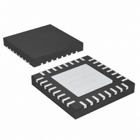
MAX16831ATJ+T Maxim Integrated Products, MAX16831ATJ+T Datasheet - Page 9

MAX16831ATJ+T
Manufacturer Part Number
MAX16831ATJ+T
Description
IC LED DRIVR HIGH BRIGHT 32-TQFN
Manufacturer
Maxim Integrated Products
Type
HBLED Driverr
Datasheet
1.MAX16831ATJT.pdf
(19 pages)
Specifications of MAX16831ATJ+T
Topology
PWM, Step-Down (Buck), Step-Up (Boost)
Number Of Outputs
1
Internal Driver
No
Type - Primary
Automotive
Type - Secondary
High Brightness LED (HBLED), RGB
Frequency
125kHz ~ 600kHz
Voltage - Supply
5.5 V ~ 76 V
Mounting Type
Surface Mount
Package / Case
32-TQFN Exposed Pad
Operating Temperature
-40°C ~ 125°C
Internal Switch(s)
Yes
Efficiency
90%
Lead Free Status / RoHS Status
Lead free / RoHS Compliant
Voltage - Output
-
Current - Output / Channel
-
Lead Free Status / Rohs Status
Details
The MAX16831 is a current-mode PWM LED driver
used for driving HBLEDs. By using two current regula-
tion loops, 5% output current accuracy is achieved.
One current regulation loop controls the external
switching MOSFET peak current through a sense resis-
tor, R
regulation loop controls the average LED string current
through the sense resistor R
The wide operating supply range of (6.0V/5.5V
ON/OFF) up to 76V makes the MAX16831 ideal in auto-
motive applications.
The MAX16831 features a programmable undervoltage
lockout (UVEN) that ensures predictable operation dur-
ing brownout conditions. The input UVEN circuit monitors
the supply voltage, V
V
V
CC
CC
PIN
drops below the UVLO threshold. Connect UVEN to
to use the 5.7V (typ) default UVLO threshold. The
25
26
27
28
29
30
31
32
—
SENSE
, from SNS+ to SNS-, while the other current
High-Voltage, High-Power LED Driver with
NAME
CLMP
REG2
CS+
V
CS-
I.C.
LO
EP
_______________________________________________________________________________________
_______________________________________________________________________________________
HI
CC
CC
Detailed Description
, and turns the driver off when
Low-Voltage Input. LO is the return point for the LED current. When using the MAX16831 in a buck-
boost configuration, connect LO to V
connect LO to SGND. Connect LO to the junction of the inductor and LED current-sense resistor,
R
Noninverting Current-Sense Amplifier Input. Connect CS+ to the positive side of an external sense
resistor, R
Inverting Current-Sense Amplifier Input. Connect CS- to the negative side of an external sense
resistor, R
Internal CLMP Regulator Output. CLMP supplies an 8V (typ) output when V
9V, V
provides the high reference for the dimming driver. V
enable the current-sense amplifier and dimming MOSFET driver. Bypass CLMP to LO with a 0.1µF
ceramic capacitor.
High-Voltage Input. HI is referred to LO. HI supplies power to the current-sense amplifier and
dimming MOSFET gate driver through the CLMP regulator.
Internal Regulator Output. REG2 is an internal voltage regulator that generates a 7V output and
supplies power to internal circuitry. Connect REG2 to DRI to power the switching MOSFET driver
during normal operation. Bypass REG2 to AGND with a 10µF ceramic capacitor.
Supply Voltage Input
Internally Connected. This pin is internally pulled to REG1 through a 10kΩ resistor. Leave this pin
unconnected or connect it to QGND using a resistor of any value. If it is directly connected to QGND,
400µA to 600µA of current will flow out of this pin from V
will reduce the current accordingly.
Exposed Pad. Connect EP to AGND. EP also functions as a heatsink to maximize thermal dissipation.
Do not use as a ground connection.
CS
CS
, when using a buck configuration.
CLMP
in series with the LEDs.
Analog and PWM Dimming Control
CS
CS
is one diode drop below V
, connected in series with the load (LEDs).
, connected in series with the load (LEDs).
CC
HI
MAX16831 includes a cycle-by-cycle current limit that
turns off the gate drive to the external switching MOS-
FET (Q
MAX16831 features a programmable oscillator that sim-
plifies and optimizes the design of external magnetics.
The MAX16831 includes three internal voltage regula-
tors, REG1, REG2, and CLMP, and a 3V buffered refer-
ence output, REF. Connect REG2 to the driver supply,
DRI, to power the switching MOSFET driver.
The MAX16831 is capable of synchronizing with an
external clock or operating in stand-alone mode. A sin-
gle resistor, R
quency from 125kHz to 600kHz for stand-alone
operation. To synchronize the device with an external
clock, apply a clock signal directly to the RTSYNC
input. A buffered clock output, CLKOUT, is available to
configure the MAX16831 in multichannel applications.
. The CLMP regulator powers the current-sense amplifier and
. When using the device in a boost configuration only,
FUNCTION
S
) during an overcurrent condition. The
Pin Description (continued)
CLMP
T
CC
, can be used to adjust the switching fre-
. Any resistor between this pin and QGND
must be at least 2.5V higher than V
HI
≥ 9V. If V
HI
is lower than
LO
to
9
9


