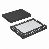
MAX16810ATU+T Maxim Integrated Products, MAX16810ATU+T Datasheet - Page 11

MAX16810ATU+T
Manufacturer Part Number
MAX16810ATU+T
Description
IC LED DRVR WT/RGB BCKLT 38-TQFN
Manufacturer
Maxim Integrated Products
Type
Backlight, White LED, RGB (Serial Interface)r
Specifications of MAX16810ATU+T
Constant Current
Yes
Topology
*
Number Of Outputs
16
Internal Driver
Yes
Type - Primary
Backlight
Type - Secondary
RGB, White LED
Frequency
20kHz ~ 1MHz
Voltage - Supply
8 V ~ 26.5 V
Voltage - Output
36V
Mounting Type
Surface Mount
Package / Case
38-TQFN Exposed Pad
Operating Temperature
-40°C ~ 125°C
Current - Output / Channel
55mA
Internal Switch(s)
No
Low Level Output Current
6 mA
High Level Output Current
1.8 mA
Operating Supply Voltage
3 V to 5.5 V
Maximum Supply Current
5 mA
Maximum Power Dissipation
2857 mW
Maximum Operating Temperature
+ 125 C
Mounting Style
SMD/SMT
Minimum Operating Temperature
- 40 C
Lead Free Status / RoHS Status
Lead free / RoHS Compliant
Efficiency
-
Lead Free Status / Rohs Status
Details
The MAX16809 LED driver includes an internal switch-
mode controller that can be used as a boost or buck-
boost (SEPIC) converter to generate the voltage
necessary to drive the multiple strings of LEDs. This
device incorporates an integrated low-side driver, a
programmable oscillator (20kHz to 1MHz), an error
amplifier, a low-voltage (300mV) current sense for high-
er efficiency, and a 5V reference to power up external
circuitry (see Figures 1a and 1b).
The MAX16809 LED driver includes a 4-wire serial
interface and a current-mode PWM controller to gener-
ate the necessary voltage for driving 16 open-drain,
constant-current-sinking output ports. The driver uses
1, 31, 32,
36, 38
16, 17
21–28
4–11
PIN
12
13
14
15
18
19
20
29
30
33
34
35
37
—
2
3
OUT8–OUT15 LED Driver Outputs. OUT8–OUT15 are open-drain, constant-current-sinking outputs rated for 36V.
OUT0–OUT7
Switch-Mode Boost and SEPIC Controller
______________________________________________________________________________________
NAME
COMP
PGND
AGND
DOUT
RTCT
N.C.
OUT
CLK
V
REF
SET
DIN
OE
V+
CS
FB
LE
EP
CC
Detailed Description
Integrated 16-Channel LED Driver with
No Connection. Not internally connected. Leave unconnected.
Error-Amplifier Inverting Input
Error-Amplifier Output
Active-Low, Output Enable Input. Drive OE low to PGND to enable the OUT0–OUT15. Drive OE
high to disable OUT0–OUT15.
Serial-Data Output. Data is clocked out of the 16-bit internal shift register to DOUT on CLK’s
rising edge.
LED Current Setting. Connect R
LED Driver Positive Supply Voltage. Bypass V+ to PGND with a 0.1μF ceramic capacitor.
Power Ground
Serial-Data Input. Data is loaded into the internal 16-bit shift register on CLK’s rising edge.
Serial-Clock Input
Latch-Enable Input. Data is loaded transparently from the internal shift register(s) to the output
latch(es) while LE is high. Data is latched into the output latch(es) on LE’s falling edge, and
retained while LE is low.
LED Driver Outputs. OUT0–OUT7 are open-drain, constant-current-sinking outputs rated for 36V.
PWM Controller Timing Resistor/Capacitor Connection. A resistor R
capacitor C
PWM Controller Current-Sense Input
Analog Ground
MOSFET Driver Output OUT. Connects to the gate of the external n-channel MOSFET.
Power-Supply Input. Bypass V
combination of a 0.1μF and a higher value ceramic capacitor.
5V Reference Output. Bypass REF to AGND with a 0.1μF ceramic capacitor.
Exposed Paddle. Connect to the ground plane for improved power dissipation. Do not use as the
only ground connection.
T
from RTCT to AGND set the oscillator frequency.
CC
SET
to AGND with a 0.1μF ceramic capacitor or a parallel
from SET to PGND to set the LED current.
current-sensing feedback circuitry (not simple current
mirrors) to ensure very small current variations over the
full allowed range of output voltage (see the Typical
Operating Characteristics ). The 4-wire serial interface
comprises a 16-bit shift register and a 16-bit transpar-
ent latch. The shift register is written through a clock
input, CLK, and a data input, DIN, and the data propa-
gates to a data output, DOUT. The data output allows
multiple drivers to be cascaded and operated together.
The contents of the 16-bit shift register are loaded into
the transparent latch through a latch-enable input, LE.
The latch is transparent to the shift register outputs
when high and latches the current state on the falling
edge of LE. Each driver output is an open-drain, con-
stant-current sink that should be connected to the
FUNCTION
T
from RTCT to REF and a
Pin Description
11


