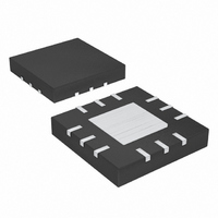
MAX1582ETC+ Maxim Integrated Products, MAX1582ETC+ Datasheet - Page 2

MAX1582ETC+
Manufacturer Part Number
MAX1582ETC+
Description
IC LED DRVR WHITE BCKLGT 12-TQFN
Manufacturer
Maxim Integrated Products
Type
Backlight, White LEDr
Datasheet
1.MAX1582ETCT.pdf
(10 pages)
Specifications of MAX1582ETC+
Constant Current
Yes
Topology
PWM, Step-Up (Boost)
Number Of Outputs
2
Internal Driver
Yes
Type - Primary
Backlight
Type - Secondary
White LED
Frequency
800kHz ~ 1.25MHz
Voltage - Supply
2.6 V ~ 5.5 V
Voltage - Output
25.5V
Mounting Type
Surface Mount
Package / Case
12-TQFN Exposed Pad
Operating Temperature
-40°C ~ 85°C
Current - Output / Channel
20mA
Internal Switch(s)
Yes
Efficiency
84%
Number Of Segments
6
Operating Supply Voltage
2.6 V to 5.5 V
Maximum Power Dissipation
1349 mW
Maximum Operating Temperature
+ 85 C
Mounting Style
SMD/SMT
Minimum Operating Temperature
- 40 C
Lead Free Status / RoHS Status
Lead free / RoHS Compliant
ABSOLUTE MAXIMUM RATINGS
V+, VP, CTRL to GND............................................-0.3V to +6.0V
PGND to GND .......................................................-0.3V to +0.3V
LX, OUT1 to GND ...................................................-0.3V to +30V
OUT2 to GND .........................................................-0.3V to +14V
COMP, CS, EN1, EN2 to GND ....................-0.3V to (V
I
High-Efficiency Step-Up Converters
for White LED Main and Subdisplay Backlighting
Stresses beyond those listed under “Absolute Maximum Ratings” may cause permanent damage to the device. These are stress ratings only, and functional
operation of the device at these or any other conditions beyond those indicated in the operational sections of the specifications is not implied. Exposure to
absolute maximum rating conditions for extended periods may affect device reliability.
ELECTRICAL CHARACTERISTICS
(V
0°C to +85°C, unless otherwise noted. Typical values are at T
2
LX ....................................................................................................
Supply Voltage
Undervoltage Lockout (UVLO)
Threshold
UVLO Hysteresis
Quiescent Current
Shutdown Supply Current
Overvoltage Lockout (OVLO)
Threshold (Rising)
OVLO Hysteresis
OUT1 Input Bias Current
Output Voltage Range (Note 2)
ERROR AMPLIFIER
CTRL to CS Regulation
CS Input Bias Current
CTRL Input Resistance
CS to COMP Transconductance
OSCILLATOR
Operating Frequency
Minimum Duty Cycle
Maximum Duty Cycle
V+
_______________________________________________________________________________________
= +3.0V, V
PARAMETER
OUT1
= 20V, L1 = 22µH, C
V+ rising or falling
No switching, V
EN1 = EN2 = GND, OUT1 = V+
MAX1582
MAX1582Y
MAX1582
MAX1582Y
MAX1582, V
MAX1582Y, V
OUT1 = V+, EN1 = EN2 = GND
MAX1582
MAX1582Y
V
V
0 < V
V
PWM mode
Pulse skipping
CTRL = V+, CS = GND
CTRL
CS
COMP
= V
CTRL
OUT
= +1.0V, V
= +1.0V
CTRL
< +1V
= 0.1µF, C
OUT1
/ 10
OUT1
CTRL
V+
V+
= +26V, EN1 = EN2 = V+
= +16V, EN1 = EN2 = V+
+ 0.3V)
1A
= +2.6V to +5.5V
= V
CONDITIONS
COMP
RMS
CS
A
= +25°C.) (Note 1)
= +0.25V
= 0.022µF, R
Continuous Power Dissipation (T
Operating Temperature Range ...........................-40°C to +85°C
Junction Temperature ......................................................+150°C
Storage Temperature Range .............................-65°C to +150°C
Lead Temperature (soldering, 10s) .................................+300°C
12-Pin Thin QFN (derate 16.9mW/°C above +70°C) ....1349mW
16-Pin UCSP (derate 6.5mW/°C above +70°C)..............518mW
SENSE
T
T
T
T
T
T
A
A
A
A
A
A
= +25°C
= +85°C
= +25°C
= +85°C
= +25°C
= +85°C
= 7.5Ω, V
CTRL
V
V
(V
(V
0.095
DIODE
DIODE
2.10
0.80
MIN
290
2.6
26
17
20
20
32
91
V+
V+
= +1.5V, EN1 = EN2 = V+, T
A
-
-
)
)
= +70°C)
0.100
TYP
2.38
0.40
0.01
0.01
0.05
0.01
500
0.1
1.3
1.0
40
27
18
40
40
50
12
94
2
1
0
0.106
MAX
2.55
0.56
25.5
17.0
1.25
780
5.5
29
19
65
65
82
1
1
1
UNITS
MHz
mV
mA
kΩ
µA
µA
µA
µS
%
%
V
V
V
V
V
V
A
=


