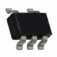
FAN5330SX Fairchild Semiconductor, FAN5330SX Datasheet - Page 6

FAN5330SX
Manufacturer Part Number
FAN5330SX
Description
IC LED DRVR WHITE BCKLGT SOT23-5
Manufacturer
Fairchild Semiconductor
Type
Backlight, White LED (Serial Interface)r
Datasheet
1.FAN5330SX.pdf
(10 pages)
Specifications of FAN5330SX
Topology
PWM, Step-Up (Boost)
Number Of Outputs
1
Internal Driver
Yes
Type - Primary
General Purpose
Frequency
1.5MHz
Voltage - Supply
1.8 V ~ 5.5 V
Voltage - Output
30V
Mounting Type
Surface Mount
Package / Case
SOT-23-5, SC-74A, SOT-25
Operating Temperature
-40°C ~ 85°C
Current - Output / Channel
35mA
Internal Switch(s)
Yes
Efficiency
88%
Operating Supply Voltage
1.8 V to 5.5 V
Maximum Operating Temperature
+ 85 C
Mounting Style
SMD/SMT
Minimum Operating Temperature
- 40 C
Lead Free Status / RoHS Status
Lead free / RoHS Compliant
Available stocks
Company
Part Number
Manufacturer
Quantity
Price
Part Number:
FAN5330SX
Manufacturer:
FAIRCHILD/ن»™ç«¥
Quantity:
20 000
Part Number:
FAN5330SX_NL
Manufacturer:
FAIRCHILD/ن»™ç«¥
Quantity:
20 000
FAN5330 Rev. 1.0.1
Block Diagram
Circuit Description
The FAN5330 is a pulse-width modulated (PWM) current-mode
boost converter. The FAN5330 improves the performance of bat-
tery powered equipment by significantly minimizing the spectral
distribution of noise at the input caused by the switching action of
the regulator. In order to facilitate effective noise filtering, the
switching frequency was chosen to be high, 1.5MHz. The device
architecture is that of a current mode controller with an internal
sense resistor connected in series with the N-channel switch.
The voltage at the feedback pin tracks the output voltage at the
cathode of the external Schottky diode (shown in the test cir-
cuit). The error amplifier amplifies the difference between the
feedback voltage and the internal bandgap reference. The
amplified error voltage serves as a reference voltage to the
PWM comparator. The inverting input of the PWM comparator
consists of the sum of two components: the amplified control
signal received from the 30m
ramp generator voltage derived from the oscillator. The oscilla-
tor sets the latch, and the latch turns on the FET switch. Under
normal operating conditions, the PWM comparator resets the
latch and turns off the FET, thus terminating the pulse. Since
the comparator input contains information about the output volt-
age and the control loop is arranged to form a negative feed-
back loop, the value of the peak inductor current will be adjusted
to maintain regulation.
Every time the latch is reset, the FET is turned off and the cur-
rent flow through the switch is terminated. The latch can be
reset by other events as well. Over-current condition is moni-
tored by the current limit comparator which resets the latch and
turns off the switch instantaneously within each clock cycle.
FB
3
Reference
Shutdown
Circuitry
SHDN
current sense resistor and the
4
-
Error
Amp
+
Generator
1.15 x V
Oscillator
Ramp
FB
REF
Shutdown
Thermal
Figure 4. Block Diagram
+
-
Over
Voltage
Comp
Current Limit
Comparator
Comp
+
V
-
5
IN
6
-
Over-Voltage Protection
The voltage on the feedback pin is sensed by an OVP Compar-
ator. When the feedback voltage is 15% higher than the nominal
voltage, the OVP Comparator stops switching of the power tran-
sistor, thus preventing the output voltage from going higher.
Open-circuit protection
As in any current regulator, if the feedback loop is open, the out-
put voltage increases until it is limited by some additional exter-
nal circuitry. In the particular case of the FAN5330, the output
voltage is limited by the switching transistor breakdown at
around 45V, typically (assuming that C
diode rating voltage are higher). Since at such high output volt-
age the output current is inherently limited by the discontinuous
conduction mode, in most cases, the switching transistor enters
non-destructive breakdown and the IC survives.
However, to ensure 100% protection for LED disconnection, we
recommend limiting V
ping the boost switching with an external voltage supervisory
circuit.
Applications Information
Setting the Output Current
The internal reference (V
current is set by a resistor divider R connected between FB pin
and ground. The output current is given by
+
R
R
R
S
Q
Driver
OUT
I
LED
with an external Zener diode or stop-
REF
=
) is 110mV (Typical). The output
Amp
V
------------- -
+
-
REF
n
R
GND
SW
2
1
30m
OUT
and the Schottky
www.fairchildsemi.com


