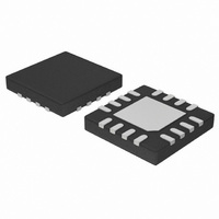
CAT3626HV4-T2 ON Semiconductor, CAT3626HV4-T2 Datasheet - Page 12

CAT3626HV4-T2
Manufacturer Part Number
CAT3626HV4-T2
Description
IC LED DRVR WT/RGB BCKLGT 16TQFN
Manufacturer
ON Semiconductor
Type
Backlight, White LED, RGB (I²C Interface)r
Datasheet
1.CAT3626HV4-GT2.pdf
(16 pages)
Specifications of CAT3626HV4-T2
Topology
PWM, Switched Capacitor (Charge Pump)
Number Of Outputs
6
Internal Driver
Yes
Type - Primary
Backlight
Type - Secondary
RGB, White LED
Frequency
800kHz ~ 1.3MHz
Voltage - Supply
3 V ~ 5.5 V
Mounting Type
Surface Mount
Package / Case
16-TFQFN Exposed Pad
Operating Temperature
-40°C ~ 85°C
Current - Output / Channel
32mA
Internal Switch(s)
Yes
Efficiency
91%
Number Of Segments
6
Operating Supply Voltage
3 V to 5.5 V
Maximum Operating Temperature
+ 85 C
Mounting Style
SMD/SMT
Minimum Operating Temperature
- 40 C
Lead Free Status / RoHS Status
Lead free / RoHS Compliant
Voltage - Output
-
Lead Free Status / Rohs Status
Lead free / RoHS Compliant
Other names
CAT3626HV4-T2CT
Available stocks
Company
Part Number
Manufacturer
Quantity
Price
Company:
Part Number:
CAT3626HV4-T2
Manufacturer:
ROHM
Quantity:
289
I
I
of the six LED channels. The SDA and SCL lines comply
with the I
terminated with pull−up resistors. When the bus is not used,
both lines are high. The device supports the maximum bus
speed of 400 kbit/s. The serial bit sequence is shown below
•
•
2
2
C Interface
C−bus in order to control the state and the current in each
S
S
The LED driver is interfaced through a 2−wire serial
Read operation:
Write operation:
Slave address
Slave address
2
SDA
C electrical specification and should be
SCL
Condition
START
Figure 27. Write Instruction Example Setting 20 mA Current in LEDB1 and LEDB2
Register address:
Slave address:
ADDRESS
1−7
W
W
R, W:
Data:
A*:
S:
A:
P:
A
A
R/W
8
Device address 7 bits (MSB first, slave address is 1100110).
Register address
Register address
Start condition
Read bit (1), Write bit (0)
Acknowledge sent by the slave LED driver (SDA high)
Not Acknowledge sent by the master microcontroller (SDA low)
Stop condition
Device register address 8 bits
Data to read or write 8 bits
Figure 26. Write Instruction Sequence
ACK
9
Figure 28. I
http://onsemi.com
1−7
ADDRESS
2
A
A
C Bus Protocol
12
8
for read and write operations into the registers. Read and
write instructions are initiated by the master controller/CPU
and acknowledged by the slave LED driver. The I
of the driver is internally fixed to the binary value 1100110.
The protocol requires that the start bit and the device address
are both repeated. For further details on the I
please refer to the I
9398 393 40011, from Philips Semiconductors.
S
Data
ACK
9
Slave address
A
1−7
2
C−Bus Specification, document number
P
DATA
R
8
A
ACK
9
Condition
Data
STOP
2
C protocol,
2
A*
C address
P


