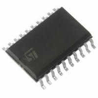
L6382D STMicroelectronics, L6382D Datasheet - Page 17

L6382D
Manufacturer Part Number
L6382D
Description
IC PFC/BALLAST CONTROLLER 20SOIC
Manufacturer
STMicroelectronics
Type
PFC/Ballast Controllerr
Datasheet
1.L6382D.pdf
(22 pages)
Specifications of L6382D
Current - Supply
2mA
Voltage - Supply
8.25 V ~ 17 V
Operating Temperature
-40°C ~ 125°C
Package / Case
20-SOIC (7.5mm Width)
Mounting Style
SMD/SMT
Lead Free Status / RoHS Status
Lead free / RoHS Compliant
Current - Output
-
Frequency
-
Lead Free Status / Rohs Status
Lead free / RoHS Compliant
Other names
497-4802-5
Available stocks
Company
Part Number
Manufacturer
Quantity
Price
Part Number:
L6382D
Manufacturer:
ST
Quantity:
20 000
Part Number:
L6382D5
Manufacturer:
ST
Quantity:
20 000
Part Number:
L6382D5TR
Manufacturer:
ST
Quantity:
20 000
Part Number:
L6382DTR
Manufacturer:
ST
Quantity:
20 000
L6382D
7.3
7.4
Drivers
●
●
●
●
●
Internal logic, over current protection (OCP) and interlocking
function
The DIM (Digital Input Monitor) block manages the input signals delivered to the drivers
ensuring that they are low during the described start-up procedure; the DIM block controls
the L6382D behaviour during both save and operating modes.
When the voltage on pin CSI overcomes the internal reference of 0.5V (typ.) the block
latches the fault condition: in this state the OCP block forces low both HSG and LSG signals
while CSO will be forced high. This condition remains latched until LSI and HSI are
simultaneously low and CSI is below 0.5V.
This function is suitable to implement an over current protection or hard-switching detection
by using an external sense resistor.
As the voltage on pin CSI can go negative, the current must be limited below 2mA by
external components.
Another feature of the DIM block is the internal interlocking that avoids cross-conduction in
the half-bridge FET's: if by chance both HGI and LGI input's are brought high at the same
time, then LSG and HSG are forced low as long as this critical condition persists.
LSD (Low Side Driver): it consists of a level shifter from 3.3V logic signal (LSI) to Vcc
MOS driving level; conceived for the half-bridge low-side power MOS, it is able to
source and sink 120mA (min).
HSD (Level Shifter and High Side Driver): it consists of a level shifter from 3.3V logic
signal (HGI) to the high side gate driver input up to 600V. Conceived for the half-bridge
high-side power MOS, the HSG is able to source and sink 120mA.
PFD (Power Factor Driver): it consists of a level shifter from 3.3V logic signal (PFI) to
Vcc MOS driving level: the driver is able to source 120mA from Vcc to PFG (turn-on)
and to sink 250mA to GND (turn-off); it is suitable to drive the MOS of the PFC pre-
regulator stage.
HED (Heat Driver): it consists of a level shifter from 3.3V logic signal (HEI) to Vcc MOS
driving level; the driver is able to source 30mA from Vcc to HEG and to sink 75mA to
GND and it is suitable for the filament heating when they are supplied by independent
winding.
Bootstrap Circuit: it generates the supply voltage for the high side Driver (HSD).
A patented integrated bootstrap section replaces an external bootstrap diode. This
section together with a bootstrap capacitor provides the bootstrap voltage to drive the
high side power MOSFET. This function is achieved using a high voltage DMOS driver
which is driven synchronously with the low side external power MOSFET. For a safe
operation, current flow between BOOT pin and Vcc is always inhibited, even though
ZVS operation may not be ensured.
Block description
17/22


