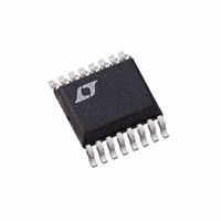
LT1768IGN Linear Technology, LT1768IGN Datasheet - Page 13

LT1768IGN
Manufacturer Part Number
LT1768IGN
Description
IC CTRLR CCFL SGL/MULT HP 16SSOP
Manufacturer
Linear Technology
Type
CCFL Controllerr
Datasheet
1.LT1768CGN.pdf
(20 pages)
Specifications of LT1768IGN
Frequency
300 ~ 410 kHz
Current - Supply
7mA
Current - Output
1.5A
Voltage - Supply
9 V ~ 24 V
Operating Temperature
-40°C ~ 125°C
Package / Case
16-SSOP
Lead Free Status / RoHS Status
Contains lead / RoHS non-compliant
Available stocks
Company
Part Number
Manufacturer
Quantity
Price
Company:
Part Number:
LT1768IGN
Manufacturer:
LT
Quantity:
10 000
Part Number:
LT1768IGN
Manufacturer:
LINEAR/凌特
Quantity:
20 000
Company:
Part Number:
LT1768IGN#PBF
Manufacturer:
LT
Quantity:
116
Part Number:
LT1768IGN#PBF
Manufacturer:
LINEAR/凌特
Quantity:
20 000
Part Number:
LT1768IGN#TRPBF
Manufacturer:
LINEAR/凌特
Quantity:
20 000
voltage and DIO lines can cause enough current flow to
fool the open lamp detection. In situations where coupling
can’t be avoided, resistors can be added from the DIO pins
to ground to increase the open lamp threshold. When
resistors from the DIO pins to ground are added, the
values for R
from their nominal values to compensate for the additional
current.
For single lamp operation, the lowside of the lamp should
be connected to both DIO pins, and the values of R
and R
used in a dual lamp configuration. In single lamp mode all
fault detection will operate as in the dual lamp configura-
tion, but the open lamp threshold will double. If the
increase in the open lamp threshold is not acceptable, a
positive offset current can be added to reduce the open
lamp threshold by placing a resistor between the REF and
DIO pins (a 33k resistor will reduce the open lamp thresh-
old by approximately 100 A ((V
an offset current is added, the values for R
may need to be increased from their nominal values to
compensate for the offset current.
VC Compensation
As previously mentioned a single capacitor on the VC pin
combines the error signal conversion, lamp current aver-
aging and frequency compensation. Careful consideration
should be given to the value of capacitance used. A large
value (1 F) will give excellent stability at high lamp cur-
rents but will result in degraded line regulation in PWM
mode. On the other hand , a small value (10nF) will give
excellent PWM response but might result in overshoot and
poor load regulation. The value chosen will depend on the
maximum load current and dimming range. After these
parameters are decided upon, the value of the VC capacitor
should be increased until the line regulation becomes
unacceptable. A typical value for the VC capacitor is
0.033 F. For further information on compensation please
refer to the references or consult the factory.
Current Sense Comparator
The LT1768 is a current mode PWM controller. Under
normal operating conditions the GATE is driven high at the
APPLICATIONS
RMIN
increased to two times the values that would be
RMAX
and R
U
RMIN
INFORMATION
U
may need to be increased
REF
W
–
V
DIO
RMAX
+
)/33k). When
and R
U
RMAX
RMIN
start of every oscillator cycle. The GATE is driven back low
when the current reaches a threshold level proportional to
the voltage on the VC pin. The GATE then remains low until
the start of the next oscillator cycle. The peak current is
thus proportional to the VC voltage and controlled on a
cycle by cycle basis. The peak switch current is normally
sensed by placing a sense resistor in the source lead of the
output MOSFET. This resistor converts the switch current
to a voltage that can be compared to a fraction of the VC
voltage [(V
GATE duty cycle below 50%, the switch current limit will
correspond to I
above 50% the switch current limit will be reduced
to approximately 90mV at 80% duty cycle to avoid
subharmonic oscillations associated with current mode
controllers.
When the lamp current is programmed to PWM mode, the
VC pin will slew between voltages that represent the
minimum and maximum PWM lamp currents. The slew
time affects the line regulation at low duty cycle, and
should be kept low by making the sense resistor as small
as possible. The lowest value of sense resistor is deter-
mined by switching transients and other noise due to
layout configurations. A good rule of thumb is to set the
sense resistor so that the voltage on the VC pin equals
2.5V when the PWM current is in maximum mode (V
= V
25m
implemented with a copper trace on the PCB.
Since the maximum threshold at the SENSE pin is only
100mV, switching transients and other noise can prema-
turely trip the comparator. The LT1768 has a blanking
period of 100ns which prohibits premature switch turn
off, but further filtering the sense resistor voltage is
recommended. A simple RC filter is adequate for most
applications. (Figure 5.)
PWM
to 50m
). Typical values of the sense resistor run in the
VC
LT1768
– V
PK
DIODE
SENSE
Figure 5. Sense Pin Filter
GATE
range for large displays, and can be
= 0.1/R
)/30] . For normal conditions and a
SENSE
2.2nF
100
. For GATE duty cycles
0.025m
LT1768
1768 •F05
13
PROG


