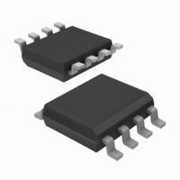
IRS2530DSPBF International Rectifier, IRS2530DSPBF Datasheet - Page 19

IRS2530DSPBF
Manufacturer Part Number
IRS2530DSPBF
Description
IC BALLAST CTRL DIM 600V 8-SOIC
Manufacturer
International Rectifier
Series
DIM8™r
Type
Ballast Controllerr
Datasheet
1.IRS2530DSTRPBF.pdf
(23 pages)
Specifications of IRS2530DSPBF
Frequency
34.2 ~ 115 kHz
Current - Supply
5mA
Current - Output
260mA
Voltage - Supply
12.5 V ~ 15.6 V
Operating Temperature
-40°C ~ 125°C
Package / Case
8-SOIC (3.9mm Width)
For Use With
IRPLDIM5E - KIT DES BALLAST 4LEVEL DIM FLUORIRPLDIM4E - KIT DES BALLAST 26W IRS2530DIRPLCFL8U - KIT DES FLUOR BALLAST IRS2530D
Lead Free Status / RoHS Status
Lead free / RoHS Compliant
Available stocks
Company
Part Number
Manufacturer
Quantity
Price
Company:
Part Number:
IRS2530DSPBF
Manufacturer:
International Rectifier
Quantity:
1 871
Company:
Part Number:
IRS2530DSPBF
Manufacturer:
IR
Quantity:
5 423
Part Number:
IRS2530DSPBF
Manufacturer:
IR
Quantity:
20 000
www.irf.com
PCB Layout Guidelines
Proper care should be taken when laying out a PCB board to minimize noise effects due to high-frequency
switching and to ensure proper functionality of the IRS2530D.
Figure 9, Typical through-hole and SMD single-layer PCB layout for Application Diagram, Page 1
(bottom copper layer shown from top view).
The programming components for the IC should be connected to the IC COM pin and then connected to
power ground at a single point (Figure 9). The lamp current sensing feedback components (RFB, CFB)
should be kept as far away as possible from the high-voltage/high-frequency half-bridge components to
prevent switching noise from distorting the lamp current feedback signal. Adjacent ground traces to the
feedback signals can also help reduce switching noise. In general, the following guidelines should be
followed during PCB board layout:
1) Place all IC supply capacitors (CVCC2, CBS) and as close as possible to their respective supply and
2) Place all IC programming and filter components as close as possible between their respective pins
3) Connect IC COM to power GND at one connection only. Do not route power GND through the
4) Connect high-side gate-drive ground (VS) to half-bridge mid-point at one connection only. Do not
5) Connect the anode of charge pump diode DCP1 to power ground. Do not connect to IC COM.
6) Use gate resistors (RLO, RHO) between all gate driver outputs and the gate of their respective
7) Use zener diode (18 V, typical) for lower charge pump diode (DCP1) and limiting resistors and
return pins (CVCC, CBS).
and COM (CVCO, RVCO, CPH, CDIM, CFB, RFB).
programming components or IC COM!
route high-side power ground through the VS components or VS pin.
power MOSFETs.
capacitors (RLIM1, CVCC1, RLIM2, CVCC2) to filter high current spikes that can cause large voltage
spikes to occur on VCC.
IC COM
connects to
Power GND
at single point
VCC charge
pump circuitry
High-side GND (VS)
connects to half-bridge
mid-point at single point
Dim
Input
CVCC1
RLIM1
DCP2
DCP1
CSNUB
(+)
(-)
RVCO
High-voltage, high-current and
high-frequency half-bridge output
RLIM2
CVCO
RLO
MLS
IC and programming
components
CPH
19
CBS
MHS
CVCC2
CDIM
1
RHO
RVCC2
CFB
Lamp current sensing
and feedback
RVCC1
(+) DC Bus
(-) DC Bus
Half-Bridge Output (VS)
RLMP2
RLMP1
RFB
Adjacent COM trace for
additional noise filtering
of feedback signal.
RCS
Power Ground
Lamp Return
Filament Sensing
© 2008 International Rectifier
IRS2530D(S)


