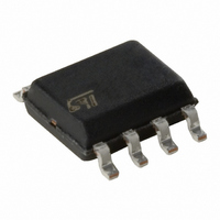
STSR2PCD-TR STMicroelectronics, STSR2PCD-TR Datasheet

STSR2PCD-TR
Specifications of STSR2PCD-TR
Available stocks
Related parts for STSR2PCD-TR
STSR2PCD-TR Summary of contents
Page 1
SUPPLY VOLTAGE RANGE: 4.5V TO 5.5V TYPICAL PEAK OUTPUT CURRENT: SOURCE -2A, SINK 3.5A OPERATING FREQUENCY 750 KHZ SMART TURN-OFF ANTICIPATION TIMING OPERATION INDEPENDENT FROM THE FORWARD MAGNETIC RESET TECHNIQUE POSSIBILITY TO OPERATE IN DISCONTINUOUS MODE DESCRIPTION STSR2P ...
Page 2
... ORDERING CODES TYPE STSR2P STSR2PM CONNECTION DIAGRAM (top view) 2/12 Parameter =105°C without heatsink A Pins 1, Pin 3 Parameter SO-8 STSR2PCD STSR2PMCD Value Unit - 270 0.9 KV -55 to +150 °C -40 to +125 °C SO-8 Unit 40 °C/W 160 °C/W SO-8 (T&R) STSR2PCD-TR STSR2PMCD-TR ...
Page 3
PIN DESCRIPTION Pin N° Symbol 1 OUT GATE1 SET ANT2 INHIBIT 6 SGLGND 7 OUT GATE2 8 PWRGND Name and Function Gate Drive signal for Rectifier MOSFET. Anticipation (t OUT is provided when ...
Page 4
STSR2P/STSR2PM ELECTRICAL CHARACTERISTICS (V otherwise specified.) Symbol Parameter SUPPLY INPUT AND UNDER VOLTAGE LOCK OUT V Start Threshold CCON V Turn OFF Threshold After CCOFF Start V Zener Voltage Z I Unloaded Supply Current CC GATE DRIVER OUTPUTS V Output ...
Page 5
TIMING DIAGRAM APPLICATION INFORMATION: STSR2 IN FORWARD CONVERTER SECONDARY SIDE NOTES 1) Ceramic Capacitors C1 and C2 must be placed very close to the IC and R2 set the anticipation time by partitioning the and ...
Page 6
STSR2P/STSR2PM EXAMPLE OF COMPONENTS SELECTION FOR A FORWARD CONVERTER Forward Specification: V =36-72V IN V =3.3V OUT n=Np/Ns=4.5 R and R are calculated assuring a minimum voltage of 2. pin. At 36V input, the voltage on the 3 ...
Page 7
INHIBIT OPERATION OF OUT NOTE: V =+200mV INHIBIT GATE2 STSR2P/STSR2PM 7/12 ...
Page 8
STSR2P/STSR2PM TYPICAL PERFORMANCE CHARACTERISTICS (unless otherwise specified T Figure 1 : Zener Characteristics Figure 2 : Rise and Fall Time vs Load Capacitor Figure 3 : OUT vs Characteristics GATE1,2 8/12 = 25°C j Figure 4 : Sink-Source ON Resistance ...
Page 9
Figure 7 : Supply Current vs Load Capacitor (each output) Figure 8 : Supply Current vs Clock Frequency Figure Temperature ON(GATE2) STSR2P/STSR2PM Figure 10 : Duty Cycle Shut Down vs Temperature Figure 11 : Duty Cycle ...
Page 10
STSR2P/STSR2PM DIM. MIN. A 1.35 A1 0.10 A2 1.10 B 0.33 C 0.19 D 4. 5.80 h 0.25 L 0.40 k ddd 10/12 SO-8 MECHANICAL DATA mm. TYP MAX. 1.75 0.25 1.65 0.51 0.25 5.00 4.00 ...
Page 11
Tape & Reel SO-8 MECHANICAL DATA mm. DIM. MIN 12 8.1 Bo 5.5 Ko 2.1 Po 3.9 P 7.9 TYP MAX. MIN. 330 13.2 0.504 0.795 2.362 22.4 8.5 0.319 5.9 0.216 ...
Page 12
... No license is granted by implication or otherwise under any patent or patent rights of STMicroelectronics. Specifications mentioned in this publication are subject to change without notice. This publication supersedes and replaces all information previously supplied ...


