IRS2111PBF International Rectifier, IRS2111PBF Datasheet
IRS2111PBF
Specifications of IRS2111PBF
Available stocks


Related parts for IRS2111PBF

IRS2111PBF Summary of contents
Page 1
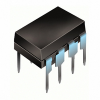
... Application Notes and DesignTips for proper circuit board layout. www.irf.com HALF-BRIDGE DRIVER Product Summary V OFFSET I +/- O V OUT t (typ.) on/off Deadtime (typ.) Packages 8-Lead PDIP IRS2111PbF Data Sheet No. PD60253 IRS2111 ( S ) PbF 600 V max. 200 mA / 420 750 ns & 150 ns 650 ns 8-Lead SOIC IRS21111SPbF up to 600 V TO ...
Page 2
Absolute Maximum Ratings Absolute maximum ratings indicate sustained limits beyond which damage to the device may occur. All voltage param- eters are absolute voltages referenced to COM. The thermal resistance and power dissipation ratings are measured under board mounted and ...
Page 3
Dynamic Electrical Characteristics 1000 pF and T BIAS are measured using the test circuit shown in Fig. 3. Symbol Definition t on Turn-on propagation delay t off ...
Page 4
Functional Block Diagram DEAD TIME UV IN DETECT DEAD TIME Lead Definitions Symbol Description IN Logic input for high-side and low-side gate driver outputs (HO & LO), in phase with HO High-side floating supply High-side gate drive ...
Page 5
Figure 1. Input/Output Timing Diagram Figure 3. Switching Time Test Circuit 50% 50% IN 90 90% Figure 5. Deadtime Waveform Definitions www.irf.com Figure 2. Floating Supply Voltage Transient Test Circuit IN (LO) 50% ...
Page 6
Temperature ( Figure 7A Turn-On Time vs Temperature 400 350 300 250 200 150 100 50 0 -50 - Temperature (°C) Figure 8A Turn-Off Time ...
Page 7
Max 50 Typ 0 -50 - Temperature (°C) Figure 10A Turn-Off Fall Time vs Temperature 1250 1000 750 500 250 0 -50 - Temperature ( Figure 11A Deadtime vs Temperature 15 ...
Page 8
Max -50 - Temperature Figure 13A Logic “0” Input voltage for HO & Logic “I” for LO vs Temperature 1.0 0.8 0.6 0.4 M ax. 0.2 Typ. 0.0 -50 -25 0 ...
Page 9
Max. 100 0 -50 - Temperature (°C) Figure 16A Offset Supply Current vs Temperature 200 150 Max. 100 Typ . 50 0 -50 - Temperature (°C) Figure 17A V Supply ...
Page 10
Max. 20 Typ. 0 -50 - Temperature (°C) Figure 19A Logic “1” Input Current vs. Temperature 6 5 Max -50 - Temperatur e (°C) ...
Page 11
Max. 9 Typ. 8 Min -50 - Temperature (°C) Figure 23 V Undervoltage (-) vs Temperature CC 500 400 Typ. 300 Min. 200 100 0 -50 - Temperature ( Figure 25A ...
Page 12
Frequency (kHz) Figure 27. IRS2111 TJ vs. Frequency (IRFBC20 GATE CC 150 125 100 1E+2 1E+3 1E+4 Frequency ...
Page 13
Frequency (kHz) Figure 31. IRS2111S TJ vs. Frequency (IRFBC20 GATE CC 150 125 100 1E+2 1E+3 1E+4 Frequency ...
Page 14
Case outlines 0.25 [.010 0.25 [.010 NOTES: 1. DIMENSIONING & TOLERANCING PER ASME Y14.5M-1994. 2. CONTROLLING ...
Page 15
Tape & Reel 8-lead SOIC NTROLLING D IM ENSION ...
Page 16
... SPN code) Assembly site code Per SCOP 200-002 ORDER INFORMATION 8-Lead PDIP IRS2111PbF 8-Lead SOIC IRS2111SPbF This product has been designed and qualified for the industrial level. Qualification standards can be found at www.irf.com Data and specifications subject to change without notice. 12/4/2006 ...