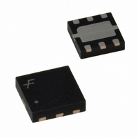
FAN3100CMPX Fairchild Semiconductor, FAN3100CMPX Datasheet - Page 15

FAN3100CMPX
Manufacturer Part Number
FAN3100CMPX
Description
IC GATE DRVR SGL CMOS 2A 6MLP
Manufacturer
Fairchild Semiconductor
Type
Low Sider
Datasheet
1.FAN3100CSX.pdf
(22 pages)
Specifications of FAN3100CMPX
Configuration
Low-Side
Input Type
Differential
Delay Time
15ns
Current - Peak
3A
Number Of Configurations
1
Number Of Outputs
1
Voltage - Supply
4.5 V ~ 18 V
Operating Temperature
-40°C ~ 125°C
Mounting Type
Surface Mount
Package / Case
6-MLP
Rise Time
20 ns
Fall Time
14 ns
Supply Voltage (min)
4.5 V
Supply Current
0.35 mA
Maximum Operating Temperature
+ 125 C
Mounting Style
SMD/SMT
Minimum Operating Temperature
- 40 C
Number Of Drivers
1
Lead Free Status / RoHS Status
Lead free / RoHS Compliant
High Side Voltage - Max (bootstrap)
-
Lead Free Status / Rohs Status
Lead free / RoHS Compliant
Other names
FAN3100CMPXTR
© 2007 Fairchild Semiconductor Corporation
FAN3100 • Rev. 1.0.3
closest to the VDD and GND pins to carry the higher-
frequency components of the current pulses.
Layout and Connection Guidelines
The FAN3100 incorporates fast reacting input circuits,
short propagation delays, and powerful output stages
capable of delivering current peaks over 2A to facilitate
voltage transition times from under 10ns to over 100ns.
The following layout and connection guidelines are
strongly recommended:
Figure 43 shows the pulsed gate drive current path
when the gate driver is supplying gate charge to turn the
MOSFET on. The current is supplied from the local
bypass capacitor, C
the MOSFET gate and to ground. To reach the high
peak currents possible, the resistance and inductance in
the path should be minimized. The localized C
contain the high peak current pulses within this driver-
MOSFET circuit, preventing them from disturbing the
sensitive analog circuitry in the PWM controller.
Keep high-current output and power ground paths
separate from logic input signals and signal ground
paths. This is especially critical when dealing with
TTL-level logic thresholds.
Keep the driver as close to the load as possible to
minimize the length of high-current traces. This
reduces the series inductance to improve high-
speed switching, while reducing the loop area that
can radiate EMI to the driver inputs and other
surrounding circuitry.
The FAN3100 is available in two packages with
slightly different pinouts, offering similar
performance. In the 6-pin MLP package, Pin 2 is
internally connected to the input analog ground and
should be connected to power ground, Pin 5,
through a short direct path underneath the IC. In the
5-pin SOT23, the internal analog and power ground
connections are made through separate, individual
bond wires to Pin 2, which should be used as the
common ground point for power and control signals.
Many high-speed power circuits can be susceptible
to noise injected from their own output or other
external sources, possibly causing output re-
triggering. These effects can be especially obvious
if the circuit is tested in breadboard or non-optimal
circuit layouts with long input, enable, or output
leads. For best results, make connections to all pins
as short and direct as possible.
The turn-on and turn-off current paths should be
minimized as discussed in the following sections.
BYP
, and flows through the driver to
BYP
acts to
15
Figure 43. Current Path for MOSFET Turn-On
www.fairchildsemi.com


