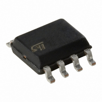
TD351ID STMicroelectronics, TD351ID Datasheet

TD351ID
Specifications of TD351ID
Available stocks
Related parts for TD351ID
TD351ID Summary of contents
Page 1
... TD351 is compatible with both pulse transformer and optocoupler signals. Applications 1200V 3-phase inverter Motor control systems UPS Order Codes Part Number Temperature Range TD351IN TD351ID -40°C, +125°C TD351IDT November 2004 Advanced IGBT/MOSFET Driver DIP-8 (Plastic Package) (Plastic Micropackage) Pin Connections (top view VREF 2 TD351 ...
Page 2
TD351 1 Block Diagram Figure 1: System and internal block diagram VH IN VREF CD LVOFF VH Table 1: Pin Description Pin Name Number IN 1 Analog input VREF 2 Analog output CD 3 Timing capacitor LVOFF 4 Analog input ...
Page 3
Absolute Maximum Ratings 2 Absolute Maximum Ratings Table 2: parameters and their absolute maximum ratings Symbol VHL Maximum Supply Voltage (VH - VL) Vout Voltage on OUT, CLAMP, LVOFF pins Vter Voltage on other pins (IN, CD, VREF) Pd Power ...
Page 4
TD351 3 Electrical Characteristics Table 4: Electrical characteristics for T Symbol Parameter Input Vton IN turn-on threshold voltage Vtoff IN turn-off threshold voltage tonmin Minimum pulse width Iinp IN Input current Voltage reference - Note 1 Vref Voltage reference Iref ...
Page 5
Functional Description 4 Functional Description 4.1 Input stage TD351 input is compatible with optocouplers or pulse transformers. The input is triggered by the signal edge and allows the use of low-sized, low- cost pulse transformer. Input is active low: output ...
Page 6
TD351 Figure 2: Detailed internal schematic Comp_Input IN 7V 1V-4V VREF 5V Vref Comp_DelayOff CD 2.5V S2 LVOFF 6/12 UVLO Filter Control Block 90uA Functional Description Comp_Clamp 2V 2-level OFF driver CLAMP VH OUT VL rev. 2 ...
Page 7
Timing Diagrams 5 Timing Diagrams Figure 3: General turn-on and 2-level turn-off sequence IN COFF Ta OUT CLAMP Vge VL level Vce Figure 4: input and output waveform dynamic parameters IN (level mode) IN (edge mode) tonmin OUT Figure 5: ...
Page 8
TD351 6 Typical Performance Curves Figure 6: Quiescent current vs temperature 2.5 2.0 1.5 1.0 0.5 0.0 -50 - Temp (°C) Figure 7: Low level output voltage vs temp. 3.0 3.0 2.0 2.0 1.0 1.0 0.0 0.0 ...
Page 9
Application Diagrams 7 Application Diagrams Figure 12: Single supply IGBT drive with active Miller clamp VH 4.7k IN VREF CD LVOFF VH Figure 13: Use of pulse transformer signals ransfo VREF CD LVOFF VH Figure 14: Large IGBT drive with ...
Page 10
TD351 8 Package Mechanical Data 8.1 DIP-8 Package DIM. MIN 0.7 B 1. 0.44 10/12 Plastic DIP-8 MECHANICAL DATA mm. TYP MAX. 3.3 1.65 ...
Page 11
Package Mechanical Data 8.2 SO-8 Package DIM. MIN. A 1.35 A1 0.10 A2 1.10 B 0.33 C 0.19 D 4. 5.80 h 0.25 L 0.40 k ddd SO-8 MECHANICAL DATA mm. TYP MAX. MIN. 1.75 0.053 ...
Page 12
... No license is granted by implication or otherwise under any patent or patent rights of STMicroelectronics. Specifications mentioned in this publication are subject to change without notice. This publication supersedes and replaces all information previously supplied. STMicroelectronics products are not authorized for use as critical components in life support devices or systems without express written approval of STMicroelectronics ...


