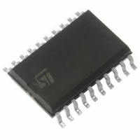
L9380-TR STMicroelectronics, L9380-TR Datasheet - Page 6

L9380-TR
Manufacturer Part Number
L9380-TR
Description
IC MOSFET DRVR TRPL HI SIDE SO20
Manufacturer
STMicroelectronics
Type
High Sider
Datasheet
1.L9380-TR.pdf
(18 pages)
Specifications of L9380-TR
Configuration
High-Side
Input Type
Non-Inverting
Current - Peak
3mA
Number Of Configurations
3
Number Of Outputs
3
Voltage - Supply
7 V ~ 18.5 V
Operating Temperature
-40°C ~ 150°C
Mounting Type
Surface Mount
Package / Case
20-SOIC (7.5mm Width)
Supply Current
2.5 mA
Maximum Operating Temperature
+ 150 C
Mounting Style
SMD/SMT
Minimum Operating Temperature
- 40 C
Number Of Drivers
3
Lead Free Status / RoHS Status
Lead free / RoHS Compliant
Delay Time
-
High Side Voltage - Max (bootstrap)
-
Lead Free Status / Rohs Status
Lead free / RoHS Compliant
Available stocks
Company
Part Number
Manufacturer
Quantity
Price
Pins description
2
Figure 2.
Table 2.
6/18
3, 13, 18
N°
10
11
12
14
15
16
17
19
20
1
2
4
5
6
7
8
9
name
GND
Pins description
Pins connection (top view)
Pins function
Pin
IN3
IN2
IN1
NC
PR
EN
G3
G2
G1
CP
S2
S1
D2
D1
T1
V
T2
S
Timer capacitor; the capacitor defines the time for the channel 1 shut down, after overload of
the external MOS transistor has been detected.
Supply voltage.
Timer capacitor; the capacitor defines the time for the channel 2 shut down, after overload of
the external MOS transistor has been detected.
Programming resistor for overload detetcion threshold; the resistor from this pin to ground
defines the drain pin current and the charging of the timer capacitor.
Input 3; equal to IN1.
Input 2; equal to IN1.
Input 1; logic signal applied to this pin controls the driver 1; this pin features a current source
to assure defined high status when the pin is open.
Enable logic signal high on this pin enables all channels
Ground
Gate 3 driver output; current source from CP or ground
Gate 2 driver output; current source from CP or ground
Source 2 sense input; monitors the source voltage.
Source 1 sense input; monitors the source voltage.
Gate 1 driver output; current source from CP or ground
Drain 2 sense input; a programmable input bias current defines the drop across the external
resistor R
Drain 1 sense input; a programmable input bias current defines the drop across the external
resistor R
Charge pump capacitor; a alternating current source at this pin charges the connected
capacitor C
to charge all the three gates of the power MOS transistors.
Not connected
D1
D1
CP
; this drop fixes the overload threshold of the external MOS.
; this drop fixes the overload threshold of the external MOS.
to a voltage 10V higher than V
GND
N.C.
IN3
IN2
IN1
VS
PR
EN
T1
T2
Doc ID 5853 Rev 3
1
2
3
4
5
6
7
8
9
10
D98AT391
Function
20
19
18
17
16
15
14
13
12
11
S
; the charge stored in this capacitor is than used
CP
D1
N.C.
D2
G1
S1
S2
N.C.
G2
G3
L9380


