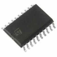
L9380 STMicroelectronics, L9380 Datasheet - Page 10

L9380
Manufacturer Part Number
L9380
Description
IC MOSFET DRVR TRPL HI SIDE SO20
Manufacturer
STMicroelectronics
Type
Triple High-Side Mosfet Driverr
Datasheet
1.L9380-TR.pdf
(18 pages)
Specifications of L9380
Configuration
High-Side
Input Type
Non-Inverting
Current - Peak
3mA
Number Of Configurations
3
Number Of Outputs
3
Voltage - Supply
7 V ~ 18.5 V
Operating Temperature
-40°C ~ 150°C
Mounting Type
Surface Mount
Package / Case
20-SOIC (7.5mm Width)
Supply Current
2.5 mA
Maximum Operating Temperature
+ 150 C
Mounting Style
SMD/SMT
Minimum Operating Temperature
- 40 C
Number Of Drivers
3
Lead Free Status / RoHS Status
Lead free / RoHS Compliant
Delay Time
-
High Side Voltage - Max (bootstrap)
-
Lead Free Status / Rohs Status
Lead free / RoHS Compliant
Available stocks
Company
Part Number
Manufacturer
Quantity
Price
Part Number:
L9380
Manufacturer:
ST
Quantity:
20 000
Functional description
10/18
In application which don’t use the overload protection or if one channel is not used, the
Timer pin of this channel must be connected to ground and the drain pin with a resistor to
V
The timing characteristic illustrates the function and the meaning of V
Figure
I
than the source pin (see
currents are equal and the half of the specified current I
equal external resistors (RD = RS) at drain and source pin are imperative. The drain sense
comparator, which detects the overload, has a symmetrical hysteresis of 20 mV (see
Figure
Exceeding the source pin voltage by 10 mV with respect to the drain voltage forces the timer
capacitor to discharge. Decreasing the source pin voltage 10 mV lower than the drain pin
voltage an overload of the external MOS is detected and the timer capacitor will be loaded.
After reaching a voltage at pin CT higher than the timer threshold V
channel is switched off. In this case the overload is stored in the timer capacitor.
The timer capacitor will be discharged with a ’High’ signal at the input (see
reaching the lower timer threshold V
able to switch on again.
Figure 3.
Figure 4.
PR
bat
+ I
.
Dmax
6). The input current of the overload sense comparator is specified as I
5).
generates a drop across the external resistor R
Timing characteristic
Drain, source input current.
I
Figure
PR
4.4V
0.4V
V
V
V
V
IN
G
S
T
+ I
Dmax
I
PR
Doc ID 5853 Rev 3
4). In the switching point the comparator input source pin
t
I
d
D
0
TLo
the overload protection is reset and the channel is
t
d
T
D98AT393
off
V
DSmin
Smax
I
D
Smax
if the drain pin voltage is higher
. For an offset compensation
D98AT392
I
S
Thi
DSmin
the influenced
Figure
and T
Smax
off
. The sum
3). After
(see
L9380


