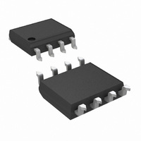
LM27222M/NOPB National Semiconductor, LM27222M/NOPB Datasheet - Page 5

LM27222M/NOPB
Manufacturer Part Number
LM27222M/NOPB
Description
IC MOSFET DVR SYNC 4.5A HS 8SOIC
Manufacturer
National Semiconductor
Datasheet
1.LM27222MXNOPB.pdf
(11 pages)
Specifications of LM27222M/NOPB
Configuration
High and Low Side, Synchronous
Input Type
PWM
Delay Time
14ns
Current - Peak
3A
Number Of Configurations
1
Number Of Outputs
2
High Side Voltage - Max (bootstrap)
30V
Voltage - Supply
4 V ~ 6.85 V
Operating Temperature
-40°C ~ 125°C
Mounting Type
Surface Mount
Package / Case
8-SOIC (3.9mm Width)
Number Of Drivers
2
Driver Configuration
Invert/Non-Invert
Driver Type
High and Low Side
Rise Time
17ns
Fall Time
14ns
Propagation Delay Time
8ns
Operating Supply Voltage (max)
6.85V
Peak Output Current
4.5mA
Power Dissipation
720mW
Operating Supply Voltage (min)
4V
Operating Temp Range
-40C to 125C
Operating Temperature Classification
Automotive
Mounting
Surface Mount
Pin Count
8
Package Type
SOIC N
Lead Free Status / RoHS Status
Lead free / RoHS Compliant
Other names
LM27222M
LOGIC
Electrical Characteristics
VCC = CB = 5V, SW = GND = 0V, unless otherwise specified. Typicals and limits appearing in plain type apply for T
+25˚C. Limits appearing in boldface type apply over the entire operating temperature range (-40˚C ≤ T
Symbol
I
Note 1: Absolute Maximum Ratings are limits beyond which damage to the device may occur. Operating ratings are conditions under which the device operates
correctly. Operating Ratings do not imply guaranteed performance limits.
Note 2: The SW pin can have -2V to -0.5 volts applied for a maximum duty cycle of 10% with a maximum period of 1 second. There is no duty cycle or maximum
period limitation for a SW pin voltage range of -0.5V to 30 Volts.
Note 3: Maximum allowable power dissipation is a function of the maximum junction temperature, T
ambient temperature, T
ambient thermal resistance, θ
θ
Note 4: Min and Max limits are 100% production tested at 25˚C. Limits over the operating temperature range are guaranteed through correlation using Statistical
Quality Control (SQC) methods. Limits are used to calculate National’s Average Outgoing Quality Level (AOQL).
Timing Diagram
V
V
leak_LEN
JA
V
V
IH_LEN
IL_LEN
IH_IN
IL_IN
for the LM27222SD is 42˚C/W. For a T
LEN pin Leakage Current
LEN Low to High Threshold
LEN High to Low Threshold
IN Low to High Threshold
IN High to Low Threshold
Threshold Hysteresis
A
. The maximum allowable power dissipation at any ambient temperature is calculated using: P
Parameter
JA
, for the LM27222M, it is 165˚C/W. For a T
JMAX
of 150˚C and TA of 25˚C, the maximum allowable power dissipation is 3W.
(Note 4) (Continued)
LEN = 0V, Source Current
LEN = 5V, Sink Current
Low to High Transition
High to Low Transition
Low to High Transition
High to Low Transition
Conditions
JMAX
of 150˚C and T
5
A
of 25˚C, the maximum allowable power dissipation is 0.76W. The
JMAX
, the junction-to-ambient thermal resistance, θ
Min
30
30
MAX
Typ
200
0.7
33
= (T
JMAX
J
≤ 125˚C).
-T
A
Max
) / θ
65
65
JA
20117904
. The junction-to-
www.national.com
A
% of V
% of V
% of V
% of V
JA
= T
Units
, and the
nA
µA
V
J
=
CC
CC
CC
CC


