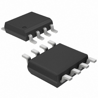
MAX4427CSA Maxim Integrated Products, MAX4427CSA Datasheet - Page 2

MAX4427CSA
Manufacturer Part Number
MAX4427CSA
Description
IC DRIVER DUAL MOSFET 1.5A 8SOIC
Manufacturer
Maxim Integrated Products
Type
Low Sider
Datasheet
1.MAX4428ESA.pdf
(7 pages)
Specifications of MAX4427CSA
Configuration
Low-Side
Input Type
Non-Inverting
Delay Time
10.0ns
Current - Peak
1.5A
Number Of Configurations
2
Number Of Outputs
2
Voltage - Supply
4.5 V ~ 18 V
Operating Temperature
0°C ~ 70°C
Mounting Type
Surface Mount
Package / Case
8-SOIC (3.9mm Width)
Rise Time
30 ns
Fall Time
30 ns
Supply Voltage (min)
4.5 V
Supply Current
4.5 mA
Maximum Power Dissipation
471 mW
Maximum Operating Temperature
+ 70 C
Mounting Style
SMD/SMT
Minimum Operating Temperature
0 C
Number Of Drivers
2
Lead Free Status / RoHS Status
Contains lead / RoHS non-compliant
High Side Voltage - Max (bootstrap)
-
Available stocks
Company
Part Number
Manufacturer
Quantity
Price
Part Number:
MAX4427CSA
Manufacturer:
MAXIM/美信
Quantity:
20 000
Company:
Part Number:
MAX4427CSA+
Manufacturer:
Maxim
Quantity:
200
Company:
Part Number:
MAX4427CSA+
Manufacturer:
AGILENT
Quantity:
115
Part Number:
MAX4427CSA+
Manufacturer:
MAXIM/美信
Quantity:
20 000
Company:
Part Number:
MAX4427CSA+T
Manufacturer:
AVAGO
Quantity:
56 000
Part Number:
MAX4427CSA+T
Manufacturer:
MAXIM/美信
Quantity:
20 000
Dual High-Speed 1.5A MOSFET Drivers
ABSOLUTE MAXIMUM RATINGS
Supply Voltage V
Time V
Input Voltage .....................................V
Continuous Power Dissipation (T
Note 1: Switching times guaranteed by design, not tested. See Figure 1 for timing measurement circuit.
Stresses beyond those listed under “Absolute Maximum Ratings” may cause permanent damage to the device. These are stress ratings only, and functional
operation of the device at these or any other conditions beyond those indicated in the operational sections of the specifications is not implied. Exposure to absolute
maximum rating conditions for extended periods may affect device reliability.
ELECTRICAL CHARACTERISTICS
(V
2
Logic 1 Input Voltage
Logic 0 Input Voltage
Input Current
Output High Voltage
Output Low Voltage
Output Resistance
Peak Output Current
Power-Supply Current
Rise Time (Note 1)
Fall Time (Note 1)
Delay Time (Note 1)
Plastic DIP (derate 9.09mW/°C above +70°C) ............727mW
SO (derate 5.88mW/°C above +70°C) ........................471mW
CERDIP (derate 8.00mW/°C above +70°C) ................640mW
DD
= +4.5V to +18V, T
IL
< V
PARAMETER
IN_
< V
DD
IH
to GND .............................................. +20V
......................................................... 50ns
A
= T
MIN
A
= +70°C)
to T
SYMBOL
I
R
V
SUPP
V
V
I
t
t
DD
V
I
OUT
MAX
PK
t
D1
D2
OH
t
IN
OL
IH
R
IL
F
+ 0.3V to GND - 0.3V
, unless otherwise specified.)
V
No load
No load
V
I
10mA
V
V
inputs
V
inputs
T
T
T
T
T
T
T
T
LOAD
A
A
A
A
A
A
A
A
IN
DD
DD
IN
IN
= +25NC
= T
= +25NC
= T
= +25NC
= T
= +25NC
= T
= 0V to 18V
= +3V for both
= 0V for both
= 18V,
= 18V
=
MIN
MIN
MIN
MIN
to T
to T
to T
to T
V
inverting stages,
V
noninverting
stages
V
inverting stages,
V
noninverting
stages
IN
IN
IN
IN
MAX
MAX
MAX
MAX
CONDITIONS
= 0.8V for
= 2.4V for
= 2.4V for
= 0.8V for
Operating Temperature Ranges:
Storage Temperature Range ............................ -55°C to +160°C
Maximum Chip Temperature ...........................................+150°C
Lead Temperature (soldering, 10 sec) ...........................+300°C
MAX442_C_ _ ..................................................... 0°C to +70°C
MAX442_E_ _ .................................................. -40°C to +85°C
MAX442_MJA .............................................. -550°C to +125°C
T
T
T
T
A
A
A
A
= +25NC
= T
= +25NC
= T
MIN
MIN
T
T
T
T
T
T
A
A
MAX
A
A
MAX
to T
to T
= +25NC
= T
= +25NC
= T
MIN
MIN
MAX
MAX
to
to
V
MIN
2.4
DD
25
-1
-
TYP
1.5
1.8
2.5
0.2
0.3
20
25
20
25
10
15
25
30
4
5
4
5
MAX
0.8
4.5
8.0
0.4
0.6
25
10
12
10
12
30
40
30
40
30
40
50
60
1
UNITS
mV
mV
mA
µA
ns
ns
ns
ns
ω
V
V
A


