MAX15024BATB+T Maxim Integrated Products, MAX15024BATB+T Datasheet - Page 2
MAX15024BATB+T
Manufacturer Part Number
MAX15024BATB+T
Description
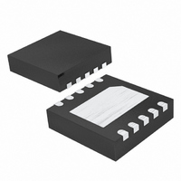
IC GATE DRVR 1CH 16NS 10TDFN-EP
Manufacturer
Maxim Integrated Products
Type
High Speedr
Datasheet
1.MAX15024AATBVT.pdf
(16 pages)
Specifications of MAX15024BATB+T
Configuration
High-Side
Input Type
Inverting and Non-Inverting
Delay Time
16ns
Current - Peak
4A
Number Of Configurations
1
Number Of Outputs
1
Voltage - Supply
6.5 V ~ 28 V
Operating Temperature
-40°C ~ 125°C
Mounting Type
Surface Mount
Package / Case
10-TDFN Exposed Pad
Rise Time
24 ns
Fall Time
16 ns
Supply Voltage (min)
6.5 V
Supply Current
1.5 mA
Maximum Power Dissipation
1481.5 mW
Maximum Operating Temperature
+ 125 C
Mounting Style
SMD/SMT
Maximum Turn-off Delay Time
18 ns
Maximum Turn-on Delay Time
18 ns
Minimum Operating Temperature
- 40 C
Number Of Drivers
1
Lead Free Status / RoHS Status
Lead free / RoHS Compliant
High Side Voltage - Max (bootstrap)
-
Lead Free Status / Rohs Status
Lead free / RoHS Compliant


ABSOLUTE MAXIMUM RATINGS
V
REG to GND ..............-0.3V to the lower of +22V or (V
DRV to PGND .........................................................-0.3V to +22V
IN_ ..........................................................................-0.3V to +22V
FB/SET to GND.........................................................-0.3V to +6V
P_OUT to DRV ........................................................-22V to +0.3V
N_OUT to PGND.....................................................-0.3V to +22V
OUT1, OUT2 to PGND ..............................-0.3V to (V
PGND to GND .......................................................-0.3V to +0.3V
P_OUT, N_OUT Continuous Source/Sink Current* .......... 200mA
OUT1, OUT2 Continuous Source/Sink Current*................200mA
Single/Dual, 16ns, High Sink/Source
Current Gate Drivers
MAX15024 ELECTRICAL CHARACTERISTICS
(V
+ 25°C). (Note 2)
* Continuous output current is limited by the power dissipation of the package.
2
Note 1: Package thermal resistances were obtained using the method described in JEDEC specification JESD51-7, using a four-
Stresses beyond those listed under “Absolute Maximum Ratings” may cause permanent damage to the device. These are stress ratings only, and functional
operation of the device at these or any other conditions beyond those indicated in the operational sections of the specifications is not implied. Exposure to
absolute maximum rating conditions for extended periods may affect device reliability.
CC
SYSTEM SPECIFICATIONS
Input Voltage Range
V
Quiescent Supply Current
Quiescent Supply Current
Under UVLO Condition
Switching Supply Current
V
V
Hysteresis
V
Output Delay
REG REGULATOR (V
Output Voltage
Dropout Voltage
Load Regulation
Line Regulation
FB/SET Reference Voltage
FB/SET Threshold
FB/SET Input Leakage Current
CC
DRV
CC
CC
CC
_______________________________________________________________________________________
to GND ............................................................-0.3V to +30V
= V
Undervoltage Lockout
Undervoltage-Lockout
Undervoltage Lockout to
Turn-On Voltage
layer board. For detailed information on package thermal considerations, see www.maxim-ic.com/thermal.tutorial.
DRV
PARAMETER
= V
REG
= 10V, FB/SET = GND, T
CC
= 12V, REG = V
UVLO_ V
SYMBOL
V
DRV
V
V
V
R
REG
CC
_
_
DO
DRV
ON
CC
, C
A
L
V
V
minimum 1µF to GND
V
V
V
IN_ = V
IN_ = V
Switching at 250kHz, C
V
V
V
12V < V
V
V
V
12V < V
External resistive divider connected at
FB/SET
V
V
= T
CC
DRV
CC
CC
CC
CC
CC
CC
CC
CC
CC
FB
FB
DRV
= 1µF, FB/SET = GND)
CC
J
falling
= 4.5V (Note 3)
= V
rising
rising
falling
powered only, V
= V
= V
= 6.5V, I
= 4.5V, I
= 12V, I
= -40°C to +125°C, unless otherwise noted. Typical values are at T
+ 0.3V)
+ 0.3V)
decoupled with
CC
CC
CC
CC
REG
REG
REG
or GND
or GND
< 28V, 0 < I
< 28V
LOAD
= V
= V
= 10V, IN+ = V
LOAD
LOAD
CONDITIONS
DRV
DRV
= 0 to 100mA
= 100mA
= 50mA
Continuous Power Dissipation (T
Junction-to-Case Thermal Resistance (Note 1) ..............8.5°C/W
Junction-to-Case Thermal Resistance (Note 1) ..............8.5°C/W
Operating Temperature Range .........................-40°C to +125°C
Junction Temperature ......................................................+150°C
Storage Temperature Range .............................-65°C to +150°C
Lead Temperature (soldering, 10s) .................................+300°C
Soldering Temperature (reflow) .......................................+260°C
(MAX15024B)
(MAX15024A)
REG
10-Pin TDFN, Single-Layer Board
(derate 18.5mW/°C above +70°C) ...........................1481.5mW
10-Pin TDFN, Multilayer Board
(derate 24.4mW/°C above +70°C) ...........................1951.2mW
LOAD
L
= 0F
=
CC
< 10mA
MAX15024B
MAX15024A
, IN- = GND
-125
MIN
1.10
6.5
4.5
6.5
4.5
3.0
9
A
= +70°C)
TYP
1.23
700
250
300
100
220
1.7
1.5
3.4
0.4
0.2
10
10
2
1
+125
MAX
1350
28.0
28.0
18.0
18.0
1.35
2.3
3.0
3.8
0.9
0.5
11
A
UNITS
= T
mA
mV
mV
mV
µA
µA
nA
µs
%
V
V
V
V
V
V
J
=
Related parts for MAX15024BATB+T
Image
Part Number
Description
Manufacturer
Datasheet
Request
R

Part Number:
Description:
(MAX15024 / MAX15025) High Sink/Source Current Gate Drivers
Manufacturer:
Maxim Integrated Products
Datasheet:
Part Number:
Description:
MAX7528KCWPMaxim Integrated Products [CMOS Dual 8-Bit Buffered Multiplying DACs]
Manufacturer:
Maxim Integrated Products
Datasheet:
Part Number:
Description:
Single +5V, fully integrated, 1.25Gbps laser diode driver.
Manufacturer:
Maxim Integrated Products
Datasheet:
Part Number:
Description:
Single +5V, fully integrated, 155Mbps laser diode driver.
Manufacturer:
Maxim Integrated Products
Datasheet:
Part Number:
Description:
VRD11/VRD10, K8 Rev F 2/3/4-Phase PWM Controllers with Integrated Dual MOSFET Drivers
Manufacturer:
Maxim Integrated Products
Datasheet:
Part Number:
Description:
Highly Integrated Level 2 SMBus Battery Chargers
Manufacturer:
Maxim Integrated Products
Datasheet:
Part Number:
Description:
Current Monitor and Accumulator with Integrated Sense Resistor; ; Temperature Range: -40°C to +85°C
Manufacturer:
Maxim Integrated Products
Part Number:
Description:
TSSOP 14/A�/RS-485 Transceivers with Integrated 100O/120O Termination Resis
Manufacturer:
Maxim Integrated Products
Part Number:
Description:
TSSOP 14/A�/RS-485 Transceivers with Integrated 100O/120O Termination Resis
Manufacturer:
Maxim Integrated Products
Part Number:
Description:
QFN 16/A�/AC-DC and DC-DC Peak-Current-Mode Converters with Integrated Step
Manufacturer:
Maxim Integrated Products
Part Number:
Description:
TDFN/A/65V, 1A, 600KHZ, SYNCHRONOUS STEP-DOWN REGULATOR WITH INTEGRATED SWI
Manufacturer:
Maxim Integrated Products
Part Number:
Description:
Integrated Temperature Controller f
Manufacturer:
Maxim Integrated Products
Part Number:
Description:
SOT23-6/I�/45MHz to 650MHz, Integrated IF VCOs with Differential Output
Manufacturer:
Maxim Integrated Products
Part Number:
Description:
SOT23-6/I�/45MHz to 650MHz, Integrated IF VCOs with Differential Output
Manufacturer:
Maxim Integrated Products
Part Number:
Description:
EVALUATION KIT/2.4GHZ TO 2.5GHZ 802.11G/B RF TRANSCEIVER WITH INTEGRATED PA
Manufacturer:
Maxim Integrated Products