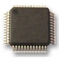
A4935KJP-T Allegro Microsystems Inc, A4935KJP-T Datasheet - Page 20

A4935KJP-T
Manufacturer Part Number
A4935KJP-T
Description
IC MOSFET DRIVER 3PH AUTO 48LQFP
Manufacturer
Allegro Microsystems Inc
Datasheet
1.A4935KJP-T.pdf
(24 pages)
Specifications of A4935KJP-T
Configuration
3 Phase Bridge
Input Type
PWM
Delay Time
90ns
Number Of Configurations
1
Number Of Outputs
3
Voltage - Supply
5.5 V ~ 50 V
Operating Temperature
-40°C ~ 150°C
Mounting Type
Surface Mount
Package / Case
48-LFQFP Exposed Pad
Device Type
Motor
Module Configuration
3-Phase Bridge
Peak Output Current
150mA
Output Resistance
8ohm
Input Delay
90ns
Output Delay
90ns
Supply Voltage Range
3V To 5.5V
Driver Case Style
LQFP
No. Of Pins
48
Operating Temperature Range
-40°C To +150°C
Rohs Compliant
Yes
Lead Free Status / RoHS Status
Lead free / RoHS Compliant
Current - Peak
-
High Side Voltage - Max (bootstrap)
-
Lead Free Status / RoHS Status
Lead free / RoHS Compliant, Lead free / RoHS Compliant
Available stocks
Company
Part Number
Manufacturer
Quantity
Price
Company:
Part Number:
A4935KJP-T
Manufacturer:
Allegro MicroSystems, LLC
Quantity:
10 000
A4935
The A4935 can also be used to perform regenerative braking.
This is equivalent to reversing the motor commutation sequence
or using fast decay with synchronous rectification. Note that
phase commutation must continue for regenerative braking to
operate and the supply must be capable of managing the reverse
current, such as by connecting a resistive load or dumping the
current to a battery or capacitor.
Current Sense Amplifier
The gain of the current sense amplifier is set using external input
and feedback resistors. Output offset can also be added using
external resistors. Care must be taken to ensure that the input
impedances seen from either end of the sense resistor match.
For the basic configuration shown in figure 4A, the two input
resistors, RN and RP, have matched values. The feedback resistor,
RF, between CSN and CSOUT, and the ground reference resis-
Figure 4. Current sense amplifier configurations
R
R
S
S
5 V
4 kΩ
4 kΩ
R
R
N
76 kΩ
P
R
G
(B) Typical Configuration
(A) Basic configuration
76 kΩ
CSN
CSP
CSN
CSP
4 kΩ
80 kΩ
R
R
F
R
G = R
G
P
A4935
= R
= R
A4935
G = 20
V
OS
F
F
N
= 250 mV
/ R
CSOUT
CSOUT
N
Automotive 3-Phase MOSFET Driver
tor, RG, between CSP and AGND also have matched values. The
gain of the sense amplfier, G, is determined by the relative values
of RF and RN, and is approximately:
If an output offset is required, for example to allow reverse cur-
rent measurement, then this can be generated by adding offset to
the CSP input through the RG resistor. Because the amplifier is
operating in a closed loop, any offset added to CSP will be mir-
rored at the output.
Figure 4B shows suitable resistor values for a gain, G, of 20 and
an output offset, V
Layout Recommendations
Careful consideration must be given to PCB layout when design-
ing high frequency, fast switching, high current circuits. The
following are recommendations regarding some of these consid-
erations:
• The A4935 analog ground, AGND, and power ground, PGND,
• The exposed thermal pad and all NC pins of the package should
• Minimize stray inductance by using short, wide copper traces at
• Consider the use of small (100 nF) ceramic decoupling
• Keep the gate discharge return connections Sx and LSS as short
should be connected together at the package pins. This common
point, and the high-current return of the external FETs, should
return separately to the negative side of the motor supply
filtering capacitor. This will minimize the effect of switching
noise on the device logic and analog reference.
be connected to the common point of AGND and PGND.
the drain and source terminals of all power FETs. This includes
motor lead connections, the input power bus, and the common
source of the low-side power FETs. This will minimize voltages
induced by fast switching of large load currents.
capacitors across the sources and drains of the power FETs to
limit fast transient voltage spikes caused by the inductance of
the circuit trace.
as possible. Any inductance on these traces will cause negative
transitions on the corresponding A4935 pins, which may exceed
the absolute maximum ratings. If this is likely, consider the use
of clamping diodes to limit the negative excursion on these pins
with respect to AGND.
OS
, of 250 mV.
G =
115 Northeast Cutoff
1.508.853.5000; www.allegromicro.com
Allegro MicroSystems, Inc.
Worcester, Massachusetts 01615-0036 U.S.A.
R
R
N
F
,
(11)
20


