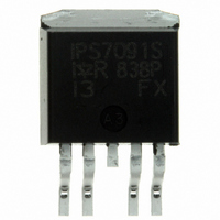
IPS7091STRLPBF International Rectifier, IPS7091STRLPBF Datasheet - Page 3

IPS7091STRLPBF
Manufacturer Part Number
IPS7091STRLPBF
Description
IC SWITCH IPS 1CH HI SIDE D2PAK
Manufacturer
International Rectifier
Type
High Sider
Datasheet
1.IPS7091STRLPBF.pdf
(15 pages)
Specifications of IPS7091STRLPBF
Input Type
Non-Inverting
Number Of Outputs
1
On-state Resistance
80 mOhm
Current - Output / Channel
1.5A
Current - Peak Output
5A
Voltage - Supply
6 V ~ 35 V
Operating Temperature
-40°C ~ 150°C
Mounting Type
Surface Mount
Package / Case
D²Pak, TO-263 (4 leads + tab)
Switch Type
High Side
Power Switch Family
IPS7091
Input Voltage
-0.3 to 5.5V
Power Switch On Resistance
90mOhm
Output Current
1.5A
Mounting
Surface Mount
Supply Current
2.5mA
Package Type
D2PAK
Operating Temperature (min)
-40C
Operating Temperature (max)
150C
Operating Temperature Classification
Automotive
Pin Count
4 +Tab
Power Dissipation
1.25W
Lead Free Status / RoHS Status
Lead free / RoHS Compliant
Other names
IPS7091STRLPBFTR
Static Electrical Characteristics
Tj=25°C, Vcc=14V (unless otherwise specified)
S
V
www.irf.com
Symbol
Rds(on)
Vcc op.
V clamp 1
V clamp 2
Vf
Icc Off
Icc On
Iout@0V
Iout@6V
Idg leakage
Vdgl
Vih
Vil
In hys
UV high
UV low
UV hys
Iin On
cc=14
Symbol
Tdon
Tr1
Tr2
dV/dt (On)
EOn
Tdoff
Tf
dV/dt (Off)
EOff
Tdiag
witc
V, Resistiv
hing E
Operating voltage range
Input low threshold voltage
Parameter
ON state resistance Tj=25°C
ON state resistance Tj=150°C
ON state resistance Tj=25°C, Vcc=6.5V
Vcc to Out clamp voltage 1
Vcc to Out clamp voltage 2
Body diode forward voltage
Supply current when Off
Supply current when On
Output leakage current
O
Diagnostic output leakage current
Low level diagnostic output voltage
Input high threshold voltage
Input hysteresis
Under voltage high threshold voltage
Under voltage low threshold voltage
U
In
Parameter
Turn-on delay time
Rise time to Vout=Vcc-5V
Rise time to Vout=0.9 x Vcc
T
T
T
Fall time to Vout=0.1 x Vcc
T
T
V
e load=14Ω, Vin=5V, Tj=25°C
urn On dV/dt
urn On energy
urn-off delay time
urn Off dV/dt
urn Off energy
ndervoltage hysteresis
out to Vdiag propagation delay
utput leakage current
put current when device is On
lectrical Characteristics
Min.
Min.
0.15
3.4
0.1
65
⎯
⎯
⎯
⎯
⎯
⎯
⎯
⎯
⎯
⎯
⎯
⎯
⎯
⎯
⎯
⎯
⎯
⎯
⎯
⎯
⎯
⎯
⎯
⎯
6
1
Typ.
Typ.
0.95
250
150
1.8
2.5
2.5
0.2
2.5
0.4
4.5
0.8
12
14
20
20
15
80
90
70
70
20
40
⎯
⎯
⎯
7
6
1
2
5
Max.
Max.
120
230
130
1.35
3.5
5.5
3.5
0.3
3.5
5.9
1.5
35
40
50
45
25
35
75
10
10
10
80
⎯
⎯
⎯
⎯
⎯
⎯
⎯
1
IPS7091(G)(S)PbF
Units
Units
V/µs
V/µs
mΩ
mA
µA
µA
µA
µs
µJ
µs
µJ
µs
V
V
Test Conditions
S
See Fig. 4 and Fig. 12
Vin=5V, Iout=2A
Iout=30mA (see Fig. 1)
Iout=1A (see Fig. 1)
Io
V
V
Vout=6V
V
V
Test Conditions
Vin=5V Iout=2A
Vin=5V, Iout=2A
Vin=5
Idg=1.6mA
ee
in=0
out=
dg=
in=
ut=
Fig. 3
5
5.5V
2.5A
V, Vout=0V
V
V
0V
,
3


