IPS6011PBF International Rectifier, IPS6011PBF Datasheet - Page 3
IPS6011PBF
Manufacturer Part Number
IPS6011PBF
Description
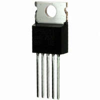
INTELLIGENT POWER SW 1CH TO220-5
Manufacturer
International Rectifier
Type
High Sider
Datasheet
1.IPS6011SPBF.pdf
(13 pages)
Specifications of IPS6011PBF
Input Type
Non-Inverting
Number Of Outputs
1
On-state Resistance
11 mOhm
Current - Output / Channel
18A
Current - Peak Output
60A
Voltage - Supply
6 V ~ 24 V
Operating Temperature
-40°C ~ 150°C
Mounting Type
Through Hole
Package / Case
TO-220-5 (Straight Leads)
Switch Type
High Side
Power Switch Family
IPS6011
Input Voltage
-0.3 to 5.5V
Power Switch On Resistance
12mOhm
Output Current
18A
Mounting
Through Hole
Supply Current
2.2mA
Package Type
TO-220
Operating Temperature (min)
-40C
Operating Temperature (max)
150C
Operating Temperature Classification
Automotive
Pin Count
5 +Tab
Power Dissipation
25W
Power Load Switch Type
High Side
Current Limit
60A
On State Resistance
0.011ohm
Thermal Protection
Yes
On / Enable Input Polarity
Active High
Power Dissipation Pd
25W
Rohs Compliant
Yes
Lead Free Status / RoHS Status
Lead free / RoHS Compliant
Available stocks
Company
Part Number
Manufacturer
Quantity
Price

Part Number:
IPS6011PBF
Manufacturer:
IR
Quantity:
20 000


Static Electrical Characteristics
Tj=25°C, Vcc=14V (unless otherwise specified)
Switching Electrical Characteristics
Vcc=14V, Resistive load=1, Vin=5V, Tj=25°C
www.irf.com
Symbol
Rds(on)
Vcc op.
V clamp 1
V clamp 2
Icc Off
Icc On
Vih
Vil
In hyst.
Iin On
Idg
Vdg
Symbol
Tdon
Tr1
Tr2
dV/dt (On)
EOn
Tdoff
Tf
dV/dt (Off)
EOff
Parameter
ON state resistance Tj=25°C
ON state resistance Tj=150°C
ON state resistance Tj=25°C, Vcc=6V
ON state resistance during reverse battery
Operating voltage range with short circuit
protection
Vcc to Out clamp voltage 1
Vcc to Out clamp voltage 2
Supply current when Off
Supply current when On
Input high threshold voltage
Input low threshold voltage
Input hysteresis
Input current when device is On
Dg leakage current
Low level DG voltage
Parameter
Turn-on delay time
Rise time to Vout=Vcc-5V
Rise time to Vout=0.9 x Vcc
Turn On dV/dt
Turn On energy
Turn-off delay time
Fall time to Vout=0.1 x Vcc
Turn Off dV/dt
Turn Off energy
Min.
Min.
1.5
0.2
37
6
Typ.
0.3
0.7
1.5
Typ.
30
25
40
70
30
19.5
0.25
4
2.2
2.5
0.5
0.1
11
12
15
39
40
40
4
2
Max.
100
140
0.8
60
50
80
Max.
2
100
2.9
0.4
14
25
17
20
24
42
10
9
5
1
IPS6011(
Units
V/µs
V/µs
mJ
mJ
Units
µs
µs
m
mA
µA
µA
V
V
V
Test Conditions
see Fig. 3
Iout=50mA
Iout=16A (see Fig. 1)
Test Conditions
Vin=5V, Iout=20A
Vin=5V, Iout=20A
Vin=5V, Iout=20A
Vcc-Gnd=14V
Vin=0V, Vout=0V
Vin=5V
Vin=5V
Vdg=5V
Idg=1.6mA
S
)(
R
)PbF
3
Related parts for IPS6011PBF
Image
Part Number
Description
Manufacturer
Datasheet
Request
R

Part Number:
Description:
SCHOTTKY RECTIFIER
Manufacturer:
International Rectifier Corp.
Datasheet:
Part Number:
Description:
SCHOTTKY RECTIFIER
Manufacturer:
International Rectifier Corp.
Datasheet:
Part Number:
Description:
SCHOTTKY RECTIFIER
Manufacturer:
International Rectifier Corp.
Datasheet:
Part Number:
Description:
SCHOTTKY RECTIFIER
Manufacturer:
International Rectifier Corp.
Datasheet:
Part Number:
Description:
SCHOTTKY RECTIFIER
Manufacturer:
International Rectifier Corp.
Datasheet:
Part Number:
Description:
SCHOTTKY RECTIFIER
Manufacturer:
International Rectifier Corp.
Datasheet:
Part Number:
Description:
SCHOTTKY RECTIFIER
Manufacturer:
International Rectifier Corp.
Datasheet:
Part Number:
Description:
SCHOTTKY RECTIFIER
Manufacturer:
International Rectifier Corp.
Datasheet:
Part Number:
Description:
SCHOTTKY RECTIFIER
Manufacturer:
International Rectifier Corp.
Datasheet:
Part Number:
Description:
SCHOTTKY RECTIFIER
Manufacturer:
International Rectifier Corp.
Datasheet:
Part Number:
Description:
SCHOTTKY RECTIFIER
Manufacturer:
International Rectifier Corp.
Datasheet:
Part Number:
Description:
SCHOTTKY RECTIFIER
Manufacturer:
International Rectifier Corp.
Datasheet:
Part Number:
Description:
SCHOTTKY RECTIFIER
Manufacturer:
International Rectifier Corp.
Datasheet:
Part Number:
Description:
SCHOTTKY RECTIFIER
Manufacturer:
International Rectifier Corp.
Datasheet:
Part Number:
Description:
SCHOTTKY RECTIFIER
Manufacturer:
International Rectifier Corp.
Datasheet: