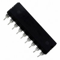
L6202 STMicroelectronics, L6202 Datasheet - Page 5

L6202
Manufacturer Part Number
L6202
Description
IC DRIVER FULL BRIDGE 18PWRDIP
Manufacturer
STMicroelectronics
Type
H Bridger
Specifications of L6202
Input Type
Non-Inverting
Number Of Outputs
2
On-state Resistance
300 mOhm
Current - Output / Channel
1.5A
Current - Peak Output
5A
Voltage - Supply
12 V ~ 48 V
Operating Temperature
-40°C ~ 150°C
Mounting Type
Through Hole
Package / Case
18-DIP (0.300", 7.62mm)
Operating Supply Voltage
12 V to 48 V
Supply Current
0.015 A
Mounting Style
Through Hole
Current, Output, High Level
2 mA
Package Type
SO20
Power Dissipation
1.3 W
Temperature, Operating, Maximum
150 °C
Temperature, Operating, Minimum
-40 °C
Voltage, Input, High Level
7 V (Max.)
Voltage, Input, Low Level
0.8 V (Max.)
Voltage, Supply
36 V (Typ.)
Lead Free Status / RoHS Status
Lead free / RoHS Compliant
Other names
497-1420-5
Available stocks
Company
Part Number
Manufacturer
Quantity
Price
Company:
Part Number:
L6202
Manufacturer:
STMicroelectronics
Quantity:
1 900
Part Number:
L6202
Manufacturer:
ST
Quantity:
20 000
ELECTRICAL CHARACTERISTICS (Continued)
LOGIC CONTROL TO POWER DRIVE TIMING
(*) Limited by power dissipation
(**) In synchronous rectification the drain-source voltage drop VDS is shown in fig. 4 (L6202/03); typical value for the L6201 is of 0.3V.
Figure 1: Typical Normalized I
Figure 3: Typical Normalized I
Symbol
t
t
t
t
t
t
t
t
1
2
3
4
5
6
7
8
(V
(V
(V
(V
(V
(V
(V
(V
i
i
i
i
i
i
i
i
)
)
)
)
)
)
)
)
Source Current Turn-off Delay
Source Current Fall Time
Source Current Turn-on Delay
Source Current Rise Time
Sink Current Turn-off Delay
Sink Current Fall Time
Sink Current Turn-on Delay
Sink Current Rise Time
Parameter
S
S
vs. T
vs. V
j
S
Fig. 12
Fig. 12
Fig. 12
Fig. 12
Fig. 13
Fig. 13
Fig. 13
Fig. 13
Test Conditions
Figure 2: Typical Normalized Quiescent Current
Figure 4: Typical R
vs. Frequency
DS (ON)
Min.
L6201 - L6202 - L6203
vs. V
Typ.
300
400
400
200
200
300
200
200
S
~ V
Max.
ref
Unit
ns
ns
ns
ns
ns
ns
ns
ns
5/20


