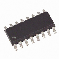
T6819-TBQ Atmel, T6819-TBQ Datasheet - Page 8

T6819-TBQ
Manufacturer Part Number
T6819-TBQ
Description
IC DRIVER DUAL TRPL DMOS 16-SOIC
Manufacturer
Atmel
Type
High Side/Low Side Driverr
Datasheet
1.T6819-TBQ.pdf
(16 pages)
Specifications of T6819-TBQ
Input Type
Serial
Number Of Outputs
6
On-state Resistance
500 mOhm
Current - Output / Channel
1.5A
Current - Peak Output
2A
Voltage - Supply
7 V ~ 40 V
Operating Temperature
-40°C ~ 150°C
Mounting Type
Surface Mount
Package / Case
16-SOIC (3.9mm Width)
For Use With
ATAB6819 - BOARD EVAL FOR T6819/ATA6829
Lead Free Status / RoHS Status
Contains lead / RoHS non-compliant
Other names
T6819-TBQTR
Noise and Surge Immunity
Note:
Electrical Characteristics
7.5 V < V
8
*) Type means: A =100% tested, B = 100% correlation tested, C = Characterized on samples, D = Design parameter
Note:
Parameters
Conducted interferences
Interference suppression
ESD (Human Body Model)
ESD (Machine Model)
No.
1.1
1.2
1.3
1.4
1.5
1.6
2.1
2.2
2.3
2.4
2.5
3.1
3.2
3.3
3.4
1
2
3
1. Test pulse 5: V
S
1. Delay time between rising edge of input signal at pin CS after data transmission and switch on/off output stages to 90% of
2. Delay time between rising/falling edge of input signal at pin PWM and switch on/off output stages to 90% of final level.
3. Difference between switch-on and switch-off delay time of input signal at pin PWM to output stages in PWM mode.
Parameters
Current Consumption
Quiescent current VS
Quiescent current VCC
Supply current VS
Supply current VCC
Discharge current VS
Discharge current VS
Undervoltage Detection, Power-on Reset
Power-on reset
threshold
Power-on reset delay
time
Undervoltage-detection
threshold
Undervoltage-detection
hysteresis
Undervoltage-detection
delay time
Thermal Prewarning and Shutdown
Thermal prewarning set
Thermal prewarning
reset
Thermal prewarning
hysteresis
Thermal shutdown off
< 40 V; 4.75 V < V
T6819/T6829 [Preliminary]
final level. Device not in standby for t > 1 ms.
smax
CC
= 40 V.
< 5.25 V; INH = High; -40° C < T
Test Conditions
V
4.75 V < V
SI = low
V
operating, all outputs
off, input register bit 13
(OLD) = high
4.75 V < V
normal operating
V
V
After switching on V
V
V
VS
VS
VS
VS
CC
CC
< 20 V, SI = low
< 20 V normal
= 32.5 V, INH = low
= 40 V, INH = low
= 5 V
= 5 V
VCC
VCC
< 5.25 V,
< 5.25 V,
Test Conditions
ISO 7637-1
VDE 0879 Part 2
ESD S 5.1
JEDEC A115A
CC
Pin
12
11
12
11
12
12
11
12
12
j
< 150° C; unless otherwise specified, all values refer to GND pins.
T
T
Symbol
T
j switch off
∆T
jPW reset
V
∆V
I
I
t
jPW set
t
V
I
VCC
I
VCC
I
I
dPor
dUV
VCC
VS
VS
VS
VS
Uv
jPW
Uv
Min.
120
105
150
0.5
2.5
3.2
5.6
30
10
Typ.
350
145
130
175
3.9
0.6
60
95
15
1
4
Max.
100
650
190
170
155
200
5.5
4.4
7.0
10
40
5
6
Level 4
Level 5
Value
200 V
2 kV
Unit
mA
mA
mA
° C
° C
° C
µA
µA
µA
µs
µs
V
V
V
K
4531D–BCD–07/04
(1)
Type*
A
A
A
A
A
A
A
A
A
A
A
B
B
B
B


