VO3120 Vishay, VO3120 Datasheet - Page 3
VO3120
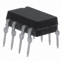
Manufacturer Part Number
VO3120
Description
IC DRIVER IGBT/MOSFET 2.5A 8-DIP
Manufacturer
Vishay
Type
High Side/Low Side Driverr
Datasheet
1.VO3120-X007T.pdf
(10 pages)
Specifications of VO3120
Isolation Voltage
5300 Vrms
Input Type
Non-Inverting
Number Of Outputs
1
Current - Output / Channel
500mA
Current - Peak Output
2.5A
Voltage - Supply
15 V ~ 32 V
Operating Temperature
-40°C ~ 110°C
Mounting Type
Through Hole
Package / Case
8-DIP (0.300", 7.62mm)
Fall Time
0.1 us
Logic Gate Type
IGBT
Rise Time
0.1 us
Configuration
1 Channel
Output Type
Integrated Photo IC
Maximum Propagation Delay Time
0.4 us
Maximum Forward Diode Voltage
1.6 V
Minimum Forward Diode Voltage
1 V
Maximum Reverse Diode Voltage
5 V
Maximum Forward Diode Current
25 mA
Maximum Continuous Output Current
2.5 A
Maximum Power Dissipation
295 mW
Maximum Operating Temperature
+ 110 C
Minimum Operating Temperature
- 40 C
No. Of Channels
1
Optocoupler Output Type
Gate Drive
Input Current
16mA
Output Voltage
500mV
Opto Case Style
DIP
No. Of Pins
8
Output Current
2.5A
Number Of Elements
1
Forward Voltage
1.6V
Forward Current
25mA
Package Type
PDIP
Power Dissipation
295mW
Propagation Delay Time
400ns
Pin Count
8
Mounting
Through Hole
Reverse Breakdown Voltage
5V
Operating Temperature Classification
Industrial
Lead Free Status / RoHS Status
Lead free / RoHS Compliant
On-state Resistance
-
Lead Free Status / Rohs Status
Compliant
Available stocks
Company
Part Number
Manufacturer
Quantity
Price

Part Number:
VO3120
Manufacturer:
VISHAY/威世
Quantity:
20 000
Part Number:
VO3120-X007
Manufacturer:
VISHAY/威世
Quantity:
20 000
Part Number:
VO3120-X007T
Manufacturer:
VISHAY/威世
Quantity:
20 000


Note
• The thermal characteristics table above were measured at 25 °C and the thermal model is represented in the thermal network below. Each
Notes
• Minimum and maximum values were tested over recommended operating conditions (T
(1)
(2)
(3)
Document Number: 81314
Rev. 1.3, 15-Mar-11
THE PRODUCT DESCRIBED HEREIN AND THIS DATASHEET ARE SUBJECT TO SPECIFIC DISCLAIMERS, SET FORTH AT
THERMAL CHARACTERISTICS
PARAMETER
LED power dissipation
Output power dissipation
Total power dissipation
Maximum LED junction temperature
Maximum output die junction temperature
Thermal resistance, junction emitter to
board
Thermal resistance, junction emitter to case
Thermal resistance, junction detector to
board
Thermal resistance, junction detector to
case
Thermal resistance, junction emitter to
junction detector
Thermal resistance, case to ambient
ELECTRICAL CHARACTERISTICS
PARAMETER
High level output current
Low level output current
High level output voltage
Low level output voltage
High level supply current
Low level supply current
Threshold input current low to high
Threshold input voltage high to low
Input forward voltage
Temperature coefficient of forward voltage
Input reverse breakdown voltage
Input capacitance
UVLO threshold
UVLO hysteresis
resistance value given in this model can be used to calculate the temperatures at each node for a given operating condition. The thermal
resistance from board to ambient will be dependent on the type of PCB, layout and thickness of copper traces. For a detailed explanation
of the thermal model, please reference Vishay's Thermal Characteristics of Optocouplers application note.
V
the result of engineering evaluations. Typical values are for information only and are not part of the testing requirements. All typical values
were measured at T
Maximum pulse width = 50 μs, maximum duty cycle = 0.5 %.
Maximum pulse width = 10 μs, maximum duty cycle = 0.2 %. This value is intended to allow for component tolerances for designs with
I
In this test V
pulse width = 1 ms, maximum duty cycle = 20 %.
O
F(OFF)
peak minimum = 2.5 A.
= - 3 V to 0.8 V, V
OH
is measured with a dc load current. When driving capacitive loads V
amb
= 25 °C and with V
CC
= 15 V to 32 V, V
For technical questions, contact:
CC
EE
2.5 A Output Current IGBT and
Output open, I
This datasheet is subject to change without notice.
SYMBOL
- V
= ground) unless otherwise specified. Typical values are characteristics of the device and are
T
T
P
P
P
EE
jmax.
jmax.
JEC
JDB
JDC
JED
diss
diss
JEB
CA
tot
V
= 32 V.
I
TEST CONDITION
f = 1 MHz, V
O
F
V
V
V
V
O
= - 3 V to + 0.8 V
= 0 mA, V
O
O
I
Output open,
O
I
O
O
= (V
I
I
I
MOSFET Driver
= (V
= (V
I
F
F
F
= (V
= - 100 mA
R
V
= 100 mA
= 10 mA
= 10 mA
= 10 mA
O
= 10 μA
F
VALUE
EE
CC
EE
5 V
2645
CC
= 7 mA to 16 mA
250
285
125
125
169
192
200
45
82
80
+ 2.5 V)
+ 15 V)
- 15 V)
- 4 V)
O
F
> 5 V
= 0 V
optocoupleranswers@vishay.com
UNIT
°C/W
°C/W
°C/W
°C/W
°C/W
°C/W
mW
mW
mW
°C
°C
SYMBOL
UVLO
V
OH
V
V
V
I
I
I
I
V
UVLO +
OH
OH
I
BV
UVLO -
OL
OL
I
I
OH
V
CCH
C
CCL
F
FLH
V
will approach V
FHL
OL
/T
IN
F
(1)
(2)
(1)
(2)
R
(3)
HYS
A
A
= - 40 °C to 110 °C, I
T
19996
V
JD
MIN.
CC
0.5
2.5
0.5
2.5
0.8
9.5
11
Vishay Semiconductors
1
5
θ
- 4
DB
CC
θ
DC
as I
OH
T
TYP.
T
- 1.4
T
B
0.2
1.6
C
60
A
θ
approaches zero A. Maximum
DE
www.vishay.com/doc?91000
T
θ
θ
A
CA
BA
F(ON)
Package
θ
EC
MAX.
13.5
θ
0.5
2.5
2.5
1.6
12
= 7 mA to 16 mA,
EB
5
www.vishay.com
VO3120
T
JE
mV/°C
UNIT
mA
mA
mA
pF
A
A
A
A
V
V
V
V
V
V
V
V
3
Related parts for VO3120
Image
Part Number
Description
Manufacturer
Datasheet
Request
R

Part Number:
Description:
357-036-542-201 CARDEDGE 36POS DL .156 BLK LOPRO
Manufacturer:
Vishay
Datasheet:
Part Number:
Description:
357-036-542-201 CARDEDGE 36POS DL .156 BLK LOPRO
Manufacturer:
Vishay
Datasheet:
Part Number:
Description:
357-036-542-201 CARDEDGE 36POS DL .156 BLK LOPRO
Manufacturer:
Vishay
Datasheet:
Part Number:
Description:
357-036-542-201 CARDEDGE 36POS DL .156 BLK LOPRO
Manufacturer:
Vishay
Datasheet:
Part Number:
Description:
357-036-542-201 CARDEDGE 36POS DL .156 BLK LOPRO
Manufacturer:
Vishay
Datasheet:
Part Number:
Description:
357-036-542-201 CARDEDGE 36POS DL .156 BLK LOPRO
Manufacturer:
Vishay
Datasheet:
Part Number:
Description:
357-036-542-201 CARDEDGE 36POS DL .156 BLK LOPRO
Manufacturer:
Vishay
Datasheet:
Part Number:
Description:
357-036-542-201 CARDEDGE 36POS DL .156 BLK LOPRO
Manufacturer:
Vishay
Datasheet:
Part Number:
Description:
357-036-542-201 CARDEDGE 36POS DL .156 BLK LOPRO
Manufacturer:
Vishay
Datasheet:
Part Number:
Description:
357-036-542-201 CARDEDGE 36POS DL .156 BLK LOPRO
Manufacturer:
Vishay
Datasheet:
Part Number:
Description:
357-036-542-201 CARDEDGE 36POS DL .156 BLK LOPRO
Manufacturer:
Vishay
Datasheet:
Part Number:
Description:
357-036-542-201 CARDEDGE 36POS DL .156 BLK LOPRO
Manufacturer:
Vishay
Datasheet:
Part Number:
Description:
357-036-542-201 CARDEDGE 36POS DL .156 BLK LOPRO
Manufacturer:
Vishay
Datasheet:
Part Number:
Description:
357-036-542-201 CARDEDGE 36POS DL .156 BLK LOPRO
Manufacturer:
Vishay
Datasheet:
Part Number:
Description:
357-036-542-201 CARDEDGE 36POS DL .156 BLK LOPRO
Manufacturer:
Vishay
Datasheet: