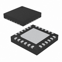
ATA6836-PXQW Atmel, ATA6836-PXQW Datasheet - Page 13

ATA6836-PXQW
Manufacturer Part Number
ATA6836-PXQW
Description
IC DVR HALF BRIDGE HEX 24-QFN
Manufacturer
Atmel
Type
Half Bridger
Datasheet
1.ATA6836-PXQW_19.pdf
(21 pages)
Specifications of ATA6836-PXQW
Input Type
Serial
Number Of Outputs
6
On-state Resistance
1.8 Ohm
Current - Peak Output
950mA
Voltage - Supply
5.5 V ~ 40 V
Operating Temperature
-40°C ~ 150°C
Mounting Type
Surface Mount
Package / Case
24-VQFN Exposed Pad, 24-HVQFN, 24-SQFN, 24-DHVQFN
Product
Half-Bridge Drivers
Rise Time
100 ns
Fall Time
100 ns
Supply Voltage (min)
3 V
Supply Current
0.15 mA
Maximum Operating Temperature
+ 150 C
Mounting Style
SMD/SMT
Bridge Type
Half Bridge
Minimum Operating Temperature
- 40 C
Number Of Drivers
6
Lead Free Status / RoHS Status
Lead free / RoHS Compliant
Current - Output / Channel
-
Lead Free Status / Rohs Status
Lead free / RoHS Compliant
Other names
ATA6836-PXSY
ATA6836-PXSY
ATA6836-PXSY
Available stocks
Company
Part Number
Manufacturer
Quantity
Price
Company:
Part Number:
ATA6836-PXQW
Manufacturer:
ATMEL
Quantity:
3 500
Part Number:
ATA6836-PXQW
Manufacturer:
ATMEL/爱特梅尔
Quantity:
20 000
7. Electrical Characteristics (Continued)
7.5V < V
4952J–AUTO–03/11
*) Type means: A = 100% tested, B = 100% correlation tested, C = Characterized on samples, D = Design parameter
Notes:
5.10
5.11
5.12
5.13
5.14
5.15
5.16
5.17
5.18
5.19
5.20
5.21
No. Parameters
5.7
5.8
5.9
6.1
6.2
6.3
6.4 Pull-down current
6
Overcurrent limitation
and shutdown threshold
Overcurrent limitation
and shutdown threshold
Overcurrent limitation
and shutdown threshold
Overcurrent shutdown
delay time
Overcurrent shutdown
delay time
High-side open load
detection current
Low-side open load
detection current
Open load detection
current ratio
High-side open load
detection voltage
Low-side open load
detection voltage
High-side output switch
on delay
Low-side output switch
on delay
High-side output switch
off delay
Low-side output switch
off delay
Dead time between
corresponding high- and
low-side switches
Inhibit Input
Input voltage low-level
threshold
Input voltage high-level
threshold
Hysteresis of input
voltage
S
1. Delay time between rising edge of input signal at pin CS after data transmission and switch on/off output stages to 90% of
< 40V; 4.75 < V
final level. Device not in standby for t > 1ms.
(1)
(1)
(1)
(1)
CC
< 5.25V; INH = High; –40°C < T
Test Conditions
V
20V < V
20V < V
Input register
bit 14 (SCT) = low
V
Input register
bit 14 (SCT) = High
V
Input register bit 13
(OLD) = low, output off
Input register bit 13
(OLD) = low, output off
Input register bit 13
(OLD) = low, output off
Input register bit 13
(OLD) = low, output off
V
R
V
R
V
R
V
R
V
R
V
VS
VS
VS
VS
VS
VS
VS
VS
INH
Load
Load
Load
Load
Load
=13V
= 13V
= 13V
= 13V
= 13V
= 13V
=13V
=13V
= V
= 30
= 30
= 30
= 30
= 30
VS
VS
VCC
< 40V
< 40V
Pin SO28 Pin QFN24
11-16,
27, 28
11-16,
27, 28
11-16,
27, 28
11-16,
27, 28
11-16,
27, 28
11-16
11-16
11-16
1-4,
1-4,
1-4,
1-4,
1-4,
1-4,
1-4,
1-4,
17
17
17
j
< 150°C; unless otherwise specified, all values refer to GND pins.
11, 20, 23
11, 20, 23
11, 20, 23
11, 20, 23
11, 20, 23
11, 20, 23
11, 20, 23
11, 20, 23
2, 5, 8,
2, 5, 8,
2, 5, 8,
2, 5, 8,
2, 5, 8,
2, 5, 8,
2, 5, 8,
2, 5, 8,
12
12
12
t
Symbol
don
V
I
I
V
I
I
OLoutLX/
OLoutHX
Out1-6H
I
I
Out1-6L
I
Out1-6H
Out1-6L
HS1-6
HS1-6
LS1-6
t
t
t
t
t
t
V
V
I
dSd
dSd
don
don
doff
doff
PD
– t
V
IH
IL
I
doff
–1400
–1600
0.3
V
Min.
1.05
650
–1.5
100
0.9
0.4
0.6
0.6
10
VCC
7
1
Typ.
–950
–950
950
1.5
1.2
12
Atmel ATA6836
0.7
Max.
–650
1600
V
–650
–0.4
700
2.1
1.5
2.5
17
20
20
20
80
VCC
2
2
3
Unit
mA
mA
mA
mA
mA
mV
ms
ms
µA
µs
µs
µs
µs
µs
V
V
V
V
Type*
C
C
A
A
A
A
A
A
A
A
A
A
A
A
A
A
A
A
13


