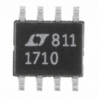
LTC1710CS8#PBF Linear Technology, LTC1710CS8#PBF Datasheet - Page 4

LTC1710CS8#PBF
Manufacturer Part Number
LTC1710CS8#PBF
Description
IC HISIDE SWTCH SMBUS DUAL 8SOIC
Manufacturer
Linear Technology
Type
High Sider
Datasheet
1.LTC1710CS8.pdf
(8 pages)
Specifications of LTC1710CS8#PBF
Input Type
2-Wire SMBus
Number Of Outputs
2
On-state Resistance
400 mOhm
Current - Output / Channel
300mA
Current - Peak Output
1A
Voltage - Supply
2.7 V ~ 5.5 V
Operating Temperature
0°C ~ 70°C
Mounting Type
Surface Mount
Package / Case
8-SOIC (3.9mm Width)
Switch Type
High Side
Power Switch Family
LTC1710
Input Voltage
2.7 to 5.5V
Power Switch On Resistance
550mOhm
Mounting
Surface Mount
Supply Current
17uA
Package Type
SOIC N
Operating Temperature (min)
0C
Operating Temperature (max)
70C
Operating Temperature Classification
Commercial
Pin Count
8
Lead Free Status / RoHS Status
Lead free / RoHS Compliant
Available stocks
Company
Part Number
Manufacturer
Quantity
Price
TYPICAL PERFOR A CE CHARACTERISTICS
PIN
LTC1710
SW0D (Pin 1): Drain Supply of Switch 0. User-program-
mable from 0V to V
OUT0 (Pin 2): Source Output of Switch 0. Maximum load
of 300mA; controlled by LSB of command byte.
AD1 (Pin 3): Three-State Programmable Address Pin.
Must be connected directly to V
two resistors 1M). Do not float this pin.
GND (Pin 4): Ground Connection.
4
0.6
1.0
0.9
0.8
0.7
0.5
0.4
0.3
0.2
0.1
50
40
30
20
10
U
0
0
– 50
– 50
Standby Current vs Temperature
Switch R
(SO-8 Package)
I
OUT
FUNCTIONS
= 300mA
U
V
V
CC
DS(ON)
V
CC
CC
TEMPERATURE ( C)
TEMPERATURE ( C)
= 2.7V
0
0
= 5V
= 3.3V
V
CC
vs Temperature
CC
= 3.3V
U
.
50
50
V
CC
V
W
CC
= 2.7V
= 5V
1710 G04
1710 G01
CC
U
100
100
, GND or V
500
400
300
200
100
1.0
0.9
0.8
0.7
0.6
0.5
0.4
0.3
0.2
0.1
0
0
– 50
CC
Supply Current (I
vs Temperature
Switch R
(MSOP Package)
0
V
I
OUT
/2 (using
CC
= 5V
= 300mA
20
DS(ON)
V
TEMPERATURE ( C)
TEMPERATURE ( C)
CC
0
BOTH SW ON
= 3.3V
40
SW1 ON
vs Temperature
Q
CLK (Pin 5): Serial Clock Interface. Must be pulled high to
V
limited to 350 A.
DATA (Pin 6): Open-Drain Connected Serial Data Inter-
face. Must be pulled high to V
pull-up current must be limited to 350 A.
OUT1 (Pin 7): Source Output of Switch 1. Maximum load
of 300mA; controlled by 2nd LSB of command byte.
V
2.7V to 5.5V.
)
CC
CC
60
50
(Pin 8): Input Supply Voltage. Operating range from
with external resistor. The pull-up current must be
SW0 ON
V
V
CC
CC
80
= 2.7V
= 5V
1710 G02
1710 G05
100
100
100
500
400
300
200
400
200
100
300
0
0
– 50
Supply Current (I
vs Supply Voltage
0
Data ACK V
T
I
A
PULL-UP
= 25 C
CC
with external resistor. The
= 350 A
2
SUPPLY VOLTAGE (V)
TEMPERATURE ( C)
OL
0
BOTH SW ON
vs Temperature
4
Q
)
50
SW1 ON
SW0 ON
6
1710 G03
1710 G06
100
8


