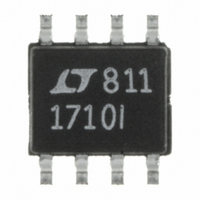
LTC1710IS8#PBF Linear Technology, LTC1710IS8#PBF Datasheet - Page 6

LTC1710IS8#PBF
Manufacturer Part Number
LTC1710IS8#PBF
Description
IC HISIDE SWTCH SMBUS DUAL 8SOIC
Manufacturer
Linear Technology
Type
High Sider
Datasheet
1.LTC1710CS8.pdf
(8 pages)
Specifications of LTC1710IS8#PBF
Input Type
2-Wire SMBus
Number Of Outputs
2
On-state Resistance
400 mOhm
Current - Output / Channel
300mA
Current - Peak Output
1A
Voltage - Supply
2.7 V ~ 5.5 V
Operating Temperature
-40°C ~ 85°C
Mounting Type
Surface Mount
Package / Case
8-SOIC (3.9mm Width)
Switch Type
High Side
Power Switch Family
LTC1710
Input Voltage
2.7 to 5.5V
Power Switch On Resistance
550mOhm
Mounting
Surface Mount
Supply Current
17uA
Package Type
SOIC N
Operating Temperature (min)
-40C
Operating Temperature (max)
85C
Operating Temperature Classification
Industrial
Pin Count
8
Lead Free Status / RoHS Status
Lead free / RoHS Compliant
Available stocks
Company
Part Number
Manufacturer
Quantity
Price
OPERATIO
LTC1710
The master then sends out the first byte. The first seven
bits of this byte consist of the address of the device that the
master wishes to communicate with. The last bit indicates
whether the command will be a read (logic one) or write
(logic zero). Because the LTC1710 is a slave device that
can only be written to by a master, it will ignore the ensuing
commands of the master if it wants to read from the
LTC1710, even if the address sent by the master matches
that of the LTC1710. After reception of the first byte, the
slave device (LTC1710) with the matching address then
acknowledges the master by pulling the DATA line low
before the next rising clock edge.
By now all other nonmatching slave devices will have gone
back to their original standby states to wait for the next
Start signal. Meanwhile, upon receiving the acknowledge
from the matching slave, the master then sends out the
command byte (see Table 1).
Table 1. Switch Control Table
COMMAND
Switch 0
Switch 1
After receiving the command byte, the slave device
(LTC1710) needs to acknowledge the master again by
pulling the DATA line low on the following clock cycle. The
master then ends this Send Byte Protocol by sending the
Stop signal, which is a transition from low to high on the
DATA line while the CLK line is high. Valid data is shifted
into the output latch on the last acknowledge signal; the
output switch will not turn on, however, until the Stop
signal is detected. This double buffering feature of the
output latch allows the user to “daisy-chain” multiple
SMBus devices such that their outputs are synchronously
6
DATA
CLK
START
XXXXXX00
START ADDR1
SW0 Off
SW1 Off
1
U
0
Example of Send Byte Protocol to Slave Address 1011000 Turning SW0 and SW1 On
A
COMMAND
XXXXXX01
SW0 On
SW1 Off
1
ADDRESS BYTE
1
A
START
XXXXXX10
(PROGRAMMABLE)
0
SW0 Off
SW1 On
ADDR2
0
A
COMMAND
Figure 1. Daisy-Chain Example
0
XXXXXX11
SW0 On
SW1 On
(WRITE)
0
A
START
ACK
ADDR3
executed on the Stop signal despite the fact that valid data
were loaded into their output latches at different times. An
example is shown in Figure 1. If somehow either the Start
or the Stop signal is detected in the middle of a byte, the
slave device (LTC1710) will regard this as an error and
reject all previous data.
Address
The LTC1710 has an address of 10110XX; the five MSBs
are hardwired, but the two LSBs are programmable by the
user with the help of a three-state address pin. Refer to
Table 2 for the pin configurations and their corresponding
addresses.
Table 2. Address Pin Truth Table
To conserve standby current, it is preferable to tie the
address pins to either V
needed, then the address pin can be tied to the third state
of V
Figure 2.
0
Figure 2. The LTC1710 Programmed with Address 1011001
A
CC
COMMAND
0
/2 by using two equal value resistors ( 1M), see
0
V
GND
AD1
V
A
CC
COMMAND BYTE
CC
STOP
/2
1710 F01
0
6
5
3
4
DATA
CLK
AD1
GND
0
LTC1710
EXECUTION OF DATA STORED IN
OUTPUT LATCH OF DEVICES WITH
ADDR1, ADDR2 AND ADDR3
CC
SW0D
OUT0
OUT1
or GND. If three LTC1710s are
V
0
CC
8
1
2
7
(SW1
ON)
1
5V
1M
1M
(SW0
ON)
1
ADDRESS
1011000
1011001
1011010
ACK
LOAD 1
LOAD 2
1710 F02
STOP
1710 TA03


