VND7N04-1-E STMicroelectronics, VND7N04-1-E Datasheet - Page 5
VND7N04-1-E
Manufacturer Part Number
VND7N04-1-E
Description
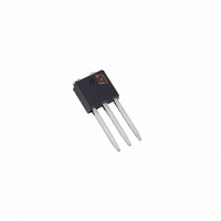
MOSFET OMNIFET 42V 7A IPAK
Manufacturer
STMicroelectronics
Series
OMNIFET II™r
Type
Low Sider
Datasheet
1.VND7N04-1-E.pdf
(17 pages)
Specifications of VND7N04-1-E
Input Type
Non-Inverting
Number Of Outputs
1
On-state Resistance
60 mOhm
Current - Peak Output
9A
Mounting Type
Through Hole
Package / Case
IPak, TO-251, DPak, VPak (3 straight leads + tab)
Lead Free Status / RoHS Status
Lead free / RoHS Compliant
Voltage - Supply
-
Operating Temperature
-
Current - Output / Channel
-
Available stocks
Company
Part Number
Manufacturer
Quantity
Price


VND7N04, VND7N04-1, VNK7N04FM
Table 5.
Table 6.
1. Pulsed: Pulse duration = 300 µs, duty cycle 1.5 %
Table 7.
Table 8.
1. Pulsed: Pulse duration = 300 µs, duty cycle 1.5 %
2. Parameters guaranteed by design/characterization
Symbol
(di/dt)on
Symbol
Symbol
Symbol
I
R
V
RRM
Q
V
t
t
t
t
g
t
d
d
d
d
C
DS(on)
SD
rr
IN(th)
fs
(on)
(off)
(on)
(off)
rr
Q
t
t
t
t
oss
r
f
r
f
(2)
(1)
i
(2)
(1)
(2)
Forward on voltage
Reverse recovery time
Reverse recovery charge
Reverse recovery current
Input threshold voltage
Static drain-source on resistance
Turn-on delay time
Rise time
Turn-off delay time
Fall time
Turn-on delay time
Rise time
Turn-off delay time
Fall time
Turn-on current slope
Total input charge
Forward
transconductance
Output capacitance
Electrical characteristics: on
Electrical characteristics: dynamic
Electrical characteristics: switching
Electrical characteristics: source drain diode
Parameter
Parameter
Parameter
Parameter
V
V
(see
V
V
(see
V
V
V
V
V
DD
gen
DD
gen
DD
in
DD
DS
DS
I
I
V
(see test circuit,
= 10 V R
SD
SD
= 15 V I
= 15 V I
= 15 V I
= 12 V I
DD
= 13 V I
= 13 V f = 1 MHz V
Figure
Figure
= 10 V R
= 10 V R
= 3.5 A V
= 3.5 A di/dt = 100 A/µs
= 30 V T
V
V
V
-40 < T
V
V
T
Test conditions
Test conditions
j
DS
in
in
in
in
= 125 ° C
= 10 V I
= 5 V I
= 10 V I
= 5 V I
Test conditions
26)
26)
gen
d
d
D
D
D
= V
gen
gen
= 3.5 A
= 3.5 A
= 3.5 A
= 3.5 A V
= 3.5 A
j
= 10
in
in
< 25 ° C
Test conditions
j
= 25 ° C
= 10
= 1000
= 0
I
D
D
D
D
D
Figure
= 3.5 A
= 3.5 A
+ I
= 3.5 A
= 3.5 A
in
in
in
= 1 mA
= 10 V
= 0
28)
Min.
Min.
2
Min.
Min.
0.8
Typ.
Typ.
250
130
140
0.4
2.5
Electrical specification
50
60
50
50
18
5
1
Typ.
0.2
3.6
40
Typ.
Max.
Max.
500
150
180
300
200
500
Max.
1.1
1.7
7
4
Max.
0.14
0.28
0.28
0.56
3
A/µs
Unit
Unit
Unit
nC
µC
pF
ns
ns
ns
ns
ns
µs
µs
µs
ns
Unit
S
V
A
V
5/17
Related parts for VND7N04-1-E
Image
Part Number
Description
Manufacturer
Datasheet
Request
R

Part Number:
Description:
MOSFET OMNIFET 42V 7A DPAK
Manufacturer:
STMicroelectronics
Datasheet:
Part Number:
Description:
MOSFET POWER 42V 7A DPAK
Manufacturer:
STMicroelectronics
Datasheet:

Part Number:
Description:
MOSFET POWER 42V 7A IPAK
Manufacturer:
STMicroelectronics
Datasheet:

Part Number:
Description:
STMicroelectronics [RIPPLE-CARRY BINARY COUNTER/DIVIDERS]
Manufacturer:
STMicroelectronics
Datasheet:
Part Number:
Description:
STMicroelectronics [LIQUID-CRYSTAL DISPLAY DRIVERS]
Manufacturer:
STMicroelectronics
Datasheet:

Part Number:
Description:
BOARD EVAL FOR MEMS SENSORS
Manufacturer:
STMicroelectronics
Datasheet:
Part Number:
Description:
NPN TRANSISTOR POWER MODULE
Manufacturer:
STMicroelectronics
Datasheet:
Part Number:
Description:
TURBOSWITCH ULTRA-FAST HIGH VOLTAGE DIODE
Manufacturer:
STMicroelectronics
Datasheet:
Part Number:
Description:
Manufacturer:
STMicroelectronics
Datasheet:
Part Number:
Description:
DIODE / SCR MODULE
Manufacturer:
STMicroelectronics
Datasheet:
Part Number:
Description:
DIODE / SCR MODULE
Manufacturer:
STMicroelectronics
Datasheet:
Part Number:
Description:
Search -----> STE16N100
Manufacturer:
STMicroelectronics
Datasheet: