VNP10N07 STMicroelectronics, VNP10N07 Datasheet - Page 2
VNP10N07
Manufacturer Part Number
VNP10N07
Description
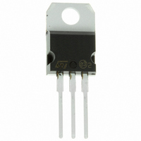
MOSFET N-CH 70V 10A TO-220
Manufacturer
STMicroelectronics
Series
OMNIFET™r
Type
Low Sider
Datasheet
1.VNP10N07.pdf
(11 pages)
Specifications of VNP10N07
Input Type
Non-Inverting
Number Of Outputs
1
On-state Resistance
100 mOhm
Current - Peak Output
10A
Mounting Type
Through Hole
Package / Case
TO-220-3 (Straight Leads)
Lead Free Status / RoHS Status
Contains lead / RoHS non-compliant
Voltage - Supply
-
Operating Temperature
-
Current - Output / Channel
-
Other names
497-2795-5
Available stocks
Company
Part Number
Manufacturer
Quantity
Price
Company:

Part Number:
VNP10N07
Manufacturer:
ST
Quantity:
5 510
Company:
Part Number:
VNP10N07
Manufacturer:
GE
Quantity:
5 510
Part Number:
VNP10N07
Manufacturer:
ST
Quantity:
20 000
Company:
Part Number:
VNP10N07-E
Manufacturer:
STMicroelectronics
Quantity:
1 800
Company:
Part Number:
VNP10N07-E
Manufacturer:
ST
Quantity:
5 000
Company:
Part Number:
VNP10N07FI
Manufacturer:
FUJI
Quantity:
6 000


VNP10N07
ABSOLUTE MAXIMUM RATING
THERMAL DATA
ELECTRICAL CHARACTERISTICS (T
OFF
ON ( )
DYNAMIC
2/11
Symbol
Symbol
Symbol
Symbol
R
R
V
R
V
g
V
V
V
V
T
thj-case
P
CLAMP
C
thj-amb
I
V
DS(on)
I
fs
T
IN(th)
I
I
T
CLTH
DSS
esd
INCL
I SS
DS
stg
D
R
tot
oss
in
c
j
( )
Drain-source Voltage (V
Input Voltage
Drain Current
Reverse DC Output Current
Electrostatic Discharge (C= 100 pF, R=1.5 K )
Total Dissipation at T
Operating Junction Temperature
Case Operating Temperature
Storage Temperature
Thermal Resistance Junction-case
Thermal Resistance Junction-ambient
Drain-source Clamp
Voltage
Drain-source Clamp
Threshold Voltage
Input-Source Reverse
Clamp Voltage
Zero Input Voltage
Drain Current (V
Supply Current from
Input Pin
Input Threshold
Voltage
Static Drain-source On
Resistance
Forward
Transconductance
Output Capacitance
Parameter
Parameter
Parameter
in
Parameter
= 0)
c
= 25
in
I
I
I
V
V
V
V
V
V
V
V
= 0)
D
D
in
DS
DS
DS
DS
in
in
DS
DS
o
= 200 mA
= 2 mA
= -1 mA
C
= 5 V
= 10 V I
= V
= 13 V
= 13 V
= 13 V
= 25 V
= 0 V
case
in
= 25
Test Conditions
Test Conditions
Test Conditions
I
I
V
V
D
D
D
f = 1 MHz
in
V
V
in
+ Ii
I
o
= 5 A
= 5 A
V
D
in
in
C unless otherwise specified)
= 0
= 10 V
in
= 5 A
= 0
= 0
n
= 0
= 1 mA
V
in
= 0
Max
Max
Internally Clamped
Internally Limited
Internally Limited
Internally Limited
-55 to 150
Min.
Min.
Min.
Value
0.8
55
2000
60
-1
6
-14
18
50
Typ.
Typ.
Typ.
62.5
250
350
2.5
70
8
Max.
Max.
Max.
0.14
-0.3
200
500
500
0.1
80
50
3
o
o
Unit
Unit
Unit
Unit
C/W
C/W
pF
o
o
o
W
V
V
V
V
S
V
V
A
A
V
C
C
C
A
A
A
Related parts for VNP10N07
Image
Part Number
Description
Manufacturer
Datasheet
Request
R

Part Number:
Description:
STMicroelectronics [RIPPLE-CARRY BINARY COUNTER/DIVIDERS]
Manufacturer:
STMicroelectronics
Datasheet:
Part Number:
Description:
STMicroelectronics [LIQUID-CRYSTAL DISPLAY DRIVERS]
Manufacturer:
STMicroelectronics
Datasheet:

Part Number:
Description:
BOARD EVAL FOR MEMS SENSORS
Manufacturer:
STMicroelectronics
Datasheet:
Part Number:
Description:
NPN TRANSISTOR POWER MODULE
Manufacturer:
STMicroelectronics
Datasheet:
Part Number:
Description:
TURBOSWITCH ULTRA-FAST HIGH VOLTAGE DIODE
Manufacturer:
STMicroelectronics
Datasheet:
Part Number:
Description:
Manufacturer:
STMicroelectronics
Datasheet:
Part Number:
Description:
DIODE / SCR MODULE
Manufacturer:
STMicroelectronics
Datasheet:
Part Number:
Description:
DIODE / SCR MODULE
Manufacturer:
STMicroelectronics
Datasheet:
Part Number:
Description:
Search -----> STE16N100
Manufacturer:
STMicroelectronics
Datasheet:
Part Number:
Description:
Search ---> STE53NA50
Manufacturer:
STMicroelectronics
Datasheet:
Part Number:
Description:
NPN Transistor Power Module
Manufacturer:
STMicroelectronics
Datasheet:
Part Number:
Description:
DIODE / SCR MODULE
Manufacturer:
STMicroelectronics
Datasheet: