VNP10N07-E STMicroelectronics, VNP10N07-E Datasheet - Page 3
VNP10N07-E
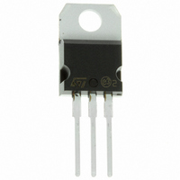
Manufacturer Part Number
VNP10N07-E
Description
MOSFET OMNIFET 70V 10A TO-220
Manufacturer
STMicroelectronics
Series
OMNIFET™r
Type
Low Sider
Datasheet
1.VNP10N07.pdf
(11 pages)
Specifications of VNP10N07-E
Input Type
Non-Inverting
Number Of Outputs
1
On-state Resistance
100 mOhm
Current - Peak Output
10A
Mounting Type
Through Hole
Package / Case
TO-220-3 (Straight Leads)
On Resistance (max)
100 mOhms
Maximum Power Dissipation
50 W
Mounting Style
Through Hole
Supply Current
0.25 mA
Transistor Polarity
N Channel
Continuous Drain Current Id
5A
Drain Source Voltage Vds
80V
On Resistance Rds(on)
100mohm
Rds(on) Test Voltage Vgs
10V
Threshold Voltage Vgs Typ
3V
Rohs Compliant
Yes
Lead Free Status / RoHS Status
Lead free / RoHS Compliant
Voltage - Supply
-
Operating Temperature
-
Current - Output / Channel
-
Lead Free Status / Rohs Status
Lead free / RoHS Compliant
Available stocks
Company
Part Number
Manufacturer
Quantity
Price
Company:

Part Number:
VNP10N07-E
Manufacturer:
STMicroelectronics
Quantity:
1 800
Company:
Part Number:
VNP10N07-E
Manufacturer:
ST
Quantity:
5 000


ELECTRICAL CHARACTERISTICS (continued)
SWITCHING ( )
SOURCE DRAIN DIODE
PROTECTION
( ) Pulsed: Pulse duration = 300 s, duty cycle 1.5 %
( ) Parameters guaranteed by design/characterization
I
t
Symbol
Symbol
Symbol
T
(di/dt)
T
E
Q
RRM
V
dlim
I
t
jsh
gf
rr
jrs
t
t
t
t
as
SD
rr
d(off)
d(off)
d(on)
d(on)
I
Q
lim
t
t
t
t
(
(
(
r
f
r
f
(
(
(
(
i
(
( )
on
)
)
)
)
)
)
)
)
Turn-on Delay Time
Rise Time
Turn-off Delay Time
Fall Time
Turn-on Delay Time
Rise Time
Turn-off Delay Time
Fall Time
Turn-on Current Slope
Total Input Charge
Forward On Voltage
Reverse Recovery
Time
Reverse Recovery
Charge
Reverse Recovery
Current
Drain Current Limit
Step Response
Current Limit
Overtemperature
Shutdown
Overtemperature Reset
Fault Sink Current
Single Pulse
Avalanche Energy
Parameter
Parameter
Parameter
V
V
(see figure 3)
V
V
(see figure 3)
V
V
V
I
I
V
(see test circuit, figure 5)
V
V
V
V
V
V
starting T
V
SD
SD
DD
gen
DD
gen
DD
in
DD
DD
in
in
in
in
in
in
in
= 5 A
= 10 V
= 5 A
= 10 V
= 5 V
= 10 V
= 5 V
= 10 V
= 5 V
= 10 V R
= 15 V
= 15 V
= 15 V
= 12 V
= 30 V
= 10 V
= 10 V
j
Test Conditions
Test Conditions
Test Conditions
= 25
V
di/dt = 100 A/ s
V
V
V
V
in
gen
I
DS
DS
D
T
DS
DS
R
I
= 0
D
j
o
R
R
= 5 A
I
I
gen
C
= 25
d
d
= 13 V
= 13 V
= 1 K
= 13 V
= 13 V
= 5 A
gen
gen
= 5 A
= 5 A
= 10
= 10
= 1000
V
o
C
DD
V
in
= 20 V
L = 10 mH
= 10 V
Min.
Min.
Min.
150
135
0.4
7
7
Typ.
Typ.
Typ.
230
100
600
125
0.9
3.8
1.7
0.3
4.8
50
80
60
30
10
10
20
50
50
20
Max.
Max.
Max.
100
160
400
180
900
2.5
1.6
14
14
30
80
2
6
VNP10N07
Unit
A/ s
Unit
Unit
mA
mA
nC
ns
ns
ns
ns
ns
ns
o
o
V
A
A
A
J
C
C
C
s
s
s
s
s
3/11
Related parts for VNP10N07-E
Image
Part Number
Description
Manufacturer
Datasheet
Request
R

Part Number:
Description:
STMicroelectronics [RIPPLE-CARRY BINARY COUNTER/DIVIDERS]
Manufacturer:
STMicroelectronics
Datasheet:
Part Number:
Description:
STMicroelectronics [LIQUID-CRYSTAL DISPLAY DRIVERS]
Manufacturer:
STMicroelectronics
Datasheet:

Part Number:
Description:
BOARD EVAL FOR MEMS SENSORS
Manufacturer:
STMicroelectronics
Datasheet:
Part Number:
Description:
NPN TRANSISTOR POWER MODULE
Manufacturer:
STMicroelectronics
Datasheet:
Part Number:
Description:
TURBOSWITCH ULTRA-FAST HIGH VOLTAGE DIODE
Manufacturer:
STMicroelectronics
Datasheet:
Part Number:
Description:
Manufacturer:
STMicroelectronics
Datasheet:
Part Number:
Description:
DIODE / SCR MODULE
Manufacturer:
STMicroelectronics
Datasheet:
Part Number:
Description:
DIODE / SCR MODULE
Manufacturer:
STMicroelectronics
Datasheet:
Part Number:
Description:
Search -----> STE16N100
Manufacturer:
STMicroelectronics
Datasheet:
Part Number:
Description:
Search ---> STE53NA50
Manufacturer:
STMicroelectronics
Datasheet:
Part Number:
Description:
NPN Transistor Power Module
Manufacturer:
STMicroelectronics
Datasheet:
Part Number:
Description:
DIODE / SCR MODULE
Manufacturer:
STMicroelectronics
Datasheet: