VND10N06 STMicroelectronics, VND10N06 Datasheet - Page 16
VND10N06
Manufacturer Part Number
VND10N06
Description
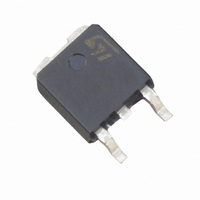
MOSFET N-CH 60V 10A DPAK
Manufacturer
STMicroelectronics
Series
OMNIFET™r
Type
Low Sider
Datasheet
1.VND10N06-1.pdf
(25 pages)
Specifications of VND10N06
Input Type
Non-Inverting
Number Of Outputs
1
On-state Resistance
150 mOhm
Current - Peak Output
10A
Mounting Type
Surface Mount
Package / Case
DPak, TO-252 (2 leads+tab), SC-63
Lead Free Status / RoHS Status
Contains lead / RoHS non-compliant
Voltage - Supply
-
Operating Temperature
-
Current - Output / Channel
-
Other names
497-2767-5
Available stocks
Company
Part Number
Manufacturer
Quantity
Price
Company:

Part Number:
VND10N06
Manufacturer:
ST
Quantity:
13 583
Company:
Part Number:
VND10N06-1
Manufacturer:
ST
Quantity:
12 500
Company:
Part Number:
VND10N06-1-E
Manufacturer:
IXYS
Quantity:
6 000
Company:
Part Number:
VND10N0613TR
Manufacturer:
ST
Quantity:
20 000
Company:
Part Number:
VND10N06TR-E
Manufacturer:
ST
Quantity:
20 000
Part Number:
VND10N06TR-E
Manufacturer:
ST
Quantity:
20 000


Protection features
3
16/25
Protection features
During normal operation, the INPUT pin is electrically connected to the gate of the internal
power MOSFET through a low impedance path as soon as V
The device then behaves like a standard power MOSFET and can be used as a switch from
DC to 50KHz. The only difference from the user’s standpoint is that a small DC current I
flows into the INPUT pin in order to supply the internal circuitry.
During turn-off of an unclamped inductive load the output voltage is clamped to a safe level
by an integrated Zener clamp between DRAIN pin and the gate of the internal Power
MOSFET.
In this condition, the Power MOSFET gate is set to a voltage high enough to sustain the
inductive load current even if the INPUT pin is driven to 0V. The device integrates an active
current limiter circuit which limits the drain current ID to Ilim whatever the INPUT pin Voltage.
When the current limiter is active, the device operates in the linear region, so power
dissipation may exceed the heatsinking capability. Both case and junction temperatures
increase, and if this phase lasts long enough, junction temperature may reach the
overtemperature threshold T
If T
restart automatically when T
j
reaches T
jsh
, the device shuts down whatever the INPUT pin voltage. The device will
j
jsh
has cooled down to T
.
jrs
.
IN
> V
VND10N06 / VND10N06-1
IH
.
ISS
Related parts for VND10N06
Image
Part Number
Description
Manufacturer
Datasheet
Request
R

Part Number:
Description:
ISO HIGH SIDE SMART POWER SOLID STATE RELAY
Manufacturer:
STMICROELECTRONICS [STMicroelectronics]
Datasheet:

Part Number:
Description:
STMicroelectronics [RIPPLE-CARRY BINARY COUNTER/DIVIDERS]
Manufacturer:
STMicroelectronics
Datasheet:
Part Number:
Description:
STMicroelectronics [LIQUID-CRYSTAL DISPLAY DRIVERS]
Manufacturer:
STMicroelectronics
Datasheet:

Part Number:
Description:
BOARD EVAL FOR MEMS SENSORS
Manufacturer:
STMicroelectronics
Datasheet:
Part Number:
Description:
NPN TRANSISTOR POWER MODULE
Manufacturer:
STMicroelectronics
Datasheet:
Part Number:
Description:
TURBOSWITCH ULTRA-FAST HIGH VOLTAGE DIODE
Manufacturer:
STMicroelectronics
Datasheet:
Part Number:
Description:
Manufacturer:
STMicroelectronics
Datasheet:
Part Number:
Description:
DIODE / SCR MODULE
Manufacturer:
STMicroelectronics
Datasheet:
Part Number:
Description:
DIODE / SCR MODULE
Manufacturer:
STMicroelectronics
Datasheet:
Part Number:
Description:
Search -----> STE16N100
Manufacturer:
STMicroelectronics
Datasheet:
Part Number:
Description:
Search ---> STE53NA50
Manufacturer:
STMicroelectronics
Datasheet:
Part Number:
Description:
NPN Transistor Power Module
Manufacturer:
STMicroelectronics
Datasheet: