VN920D-B5 STMicroelectronics, VN920D-B5 Datasheet - Page 5
VN920D-B5
Manufacturer Part Number
VN920D-B5
Description
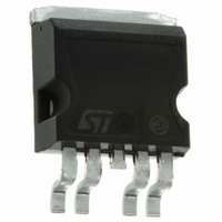
IC DRIVER HIGH SIDE P2PAK
Manufacturer
STMicroelectronics
Type
High Sider
Datasheet
1.VN920D-B513TR.pdf
(32 pages)
Specifications of VN920D-B5
Input Type
Non-Inverting
Number Of Outputs
1
On-state Resistance
18 mOhm
Current - Output / Channel
45A
Voltage - Supply
5.5 V ~ 36 V
Operating Temperature
-40°C ~ 150°C
Mounting Type
Surface Mount
Package / Case
P²PAK (4 leads + Tab)
Switch Type
High Side
Power Switch Family
VN920D-B5
Power Switch On Resistance
50mOhm
Mounting
Surface Mount
Supply Current
10uA
Package Type
P2PAK
Operating Temperature (min)
-40C
Operating Temperature (max)
150C
Operating Temperature Classification
Automotive
Pin Count
4 +Tab
Power Dissipation
96.1W
Lead Free Status / RoHS Status
Lead free / RoHS Compliant
Current - Peak Output
-
Lead Free Status / Rohs Status
Not Compliant
Available stocks
Company
Part Number
Manufacturer
Quantity
Price

Part Number:
VN920D-B5
Manufacturer:
ST
Quantity:
20 000


VN920D-B5 / VN920DSO
1
Block diagram and pin description
Figure 1.
Figure 2.
Table 2.
Connection / pin
STATUS
To ground
GND
INPUT
Floating
Block diagram
Configuration diagram (top view)
Suggested connections for unused and not connected pins
OVER-TEMPERATURE
DETECTION
P2PAK
V
CLAMP
CC
Status
5
4
3
2
1
X
OUTPUT
STATUS
V
INPUT
GND
CC
LOGIC
N.C.
X
X
AND OUTPUT SHORTED TO V
OVER-VOLTAGE
DETECTION
UNDER-VOLTAGE
DRIVER
ON
OFF
CURRENT LIMITER
DETECTION
-
STATE OPEN LOAD
-
STATE OPEN LOAD
V
GND
INPUT
V
N.C.
STATUS
N.C.
N.C.
DETECTION
Output
DETECTION
CC
CC
Block diagram and pin description
X
Power CLAMP
1
8
SO-16L
Through 10KΩ resistor
CC
16
9
OUTPUT
V
OUTPUT
OUTPUT
OUTPUT
OUTPUT
OUTPUT
V
Input
CC
CC
X
V
CC
OUTPUT
5/32
Related parts for VN920D-B5
Image
Part Number
Description
Manufacturer
Datasheet
Request
R

Part Number:
Description:
HIGH SIDE DRIVER
Manufacturer:
STMICROELECTRONICS [STMicroelectronics]
Datasheet:

Part Number:
Description:
IC DRIVER HIGHSIDE 1CH P2PAK-4
Manufacturer:
STMicroelectronics
Datasheet:

Part Number:
Description:
High Side Driver
Manufacturer:
STMicroelectronics
Datasheet:

Part Number:
Description:
IC DRIVER SINGLE 30A PENTAWATT
Manufacturer:
STMicroelectronics
Datasheet:
Part Number:
Description:
IC DRIVER SINGLE 30A P2-PAK
Manufacturer:
STMicroelectronics
Datasheet:
Part Number:
Description:
IC SSR HIGHSIDE 1CH P2PAK-4
Manufacturer:
STMicroelectronics
Datasheet:
Part Number:
Description:
IC DRIVER HIGH SIDE PENTAWATT-5
Manufacturer:
STMicroelectronics
Datasheet:
Part Number:
Description:
IC SSR HIGH SIDE SGL CHAN P2PAK
Manufacturer:
STMicroelectronics
Datasheet:
Part Number:
Description:
IC SSR HIGHSIDE 1CH PENTAWATT5
Manufacturer:
STMicroelectronics
Datasheet:
Part Number:
Description:
IC DRIVER HIGH SIDE PENTAWATT-5
Manufacturer:
STMicroelectronics
Datasheet:
Part Number:
Description:
Single Channel High Side Solid State Relay
Manufacturer:
STMicroelectronics
Datasheet:
Part Number:
Description:
STMicroelectronics [RIPPLE-CARRY BINARY COUNTER/DIVIDERS]
Manufacturer:
STMicroelectronics
Datasheet:
Part Number:
Description:
STMicroelectronics [LIQUID-CRYSTAL DISPLAY DRIVERS]
Manufacturer:
STMicroelectronics
Datasheet:

Part Number:
Description:
BOARD EVAL FOR MEMS SENSORS
Manufacturer:
STMicroelectronics
Datasheet: