VN920SP STMicroelectronics, VN920SP Datasheet - Page 17
VN920SP
Manufacturer Part Number
VN920SP
Description
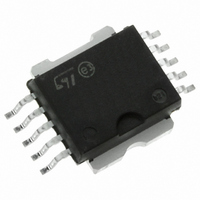
IC SSR HIGHSIDE 1CH POWERSO10
Manufacturer
STMicroelectronics
Type
High Sider
Datasheet
1.VN920SP13TR.pdf
(26 pages)
Specifications of VN920SP
Input Type
Non-Inverting
Number Of Outputs
1
On-state Resistance
15 mOhm
Current - Output / Channel
45A
Voltage - Supply
5.5 V ~ 36 V
Operating Temperature
-40°C ~ 150°C
Mounting Type
Surface Mount
Package / Case
PowerSO-10 Exposed Bottom Pad
Lead Free Status / RoHS Status
Lead free / RoHS Compliant
Current - Peak Output
-
Available stocks
Company
Part Number
Manufacturer
Quantity
Price
Company:

Part Number:
VN920SP
Manufacturer:
ST
Quantity:
12 388
Part Number:
VN920SP
Manufacturer:
ST
Quantity:
20 000
Part Number:
VN920SP-E
Manufacturer:
ST
Quantity:
20 000
Part Number:
VN920SPTR-E
Manufacturer:
ST
Quantity:
20 000
Company:
Part Number:
VN920SPTRE
Manufacturer:
INTEL
Quantity:
3 054


VN920SP
3.1.2
3.2
3.3
Solution 2: diode (D
A resistor (R
inductive load.
This small signal diode can be safely shared amongst several different HSDs. Also in this
case, the presence of the ground network will produce a shift ( 600mV) in the input
threshold and in the status output values if the microprocessor ground is not common to the
device ground. This shift will not vary if more than one HSD shares the same diode/resistor
network.
Series resistor in INPUT and STATUS lines are also required to prevent that, during battery
voltage transient, the current exceeds the absolute maximum rating.
Safest configuration for unused INPUT and STATUS pin is to leave them unconnected.
Load dump protection
D
V
that are greater than the ones shown in the ISO 7637-2: 2004(E) table.
MCU I/Os protection
If a ground protection network is used and negative transient are present on the V
the control pins will be pulled negative. ST suggests to insert a resistor (R
prevent the µC I/Os pins to latch-up.
The value of these resistors is a compromise between the leakage current of C and the
current required by the HSD I/Os (Input levels compatibility) with the latch-up limit of C
I/Os.
-V
Calculation example:
For V
5k
Recommended values: R
CC
ld
CCpeak
is necessary (Voltage Transient Suppressor) if the load dump peak voltage exceeds the
max DC rating. The same applies if the device is subject to transients on the V
CCpeak
R
prot
/I
latchup
65k .
= - 100V and I
GND
= 1k
R
prot
(V
should be inserted in parallel to D
prot
GND
OH
latchup
µ
=10k .
C
) in the ground line
-V
IH
20mA; V
-V
GND
) / I
OH
IHmax
µ
C
4.5V
GND
if the device drives an
Application information
prot
) in line to
CC
CC
line,
line
17/26
Related parts for VN920SP
Image
Part Number
Description
Manufacturer
Datasheet
Request
R

Part Number:
Description:
IC DRIVER SINGLE 30A PENTAWATT
Manufacturer:
STMicroelectronics
Datasheet:

Part Number:
Description:
IC DRIVER SINGLE 30A P2-PAK
Manufacturer:
STMicroelectronics
Datasheet:
Part Number:
Description:
IC SSR HIGHSIDE 1CH P2PAK-4
Manufacturer:
STMicroelectronics
Datasheet:
Part Number:
Description:
IC DRIVER HIGH SIDE PENTAWATT-5
Manufacturer:
STMicroelectronics
Datasheet:

Part Number:
Description:
IC SSR HIGH SIDE SGL CHAN P2PAK
Manufacturer:
STMicroelectronics
Datasheet:
Part Number:
Description:
IC SSR HIGHSIDE 1CH PENTAWATT5
Manufacturer:
STMicroelectronics
Datasheet:
Part Number:
Description:
IC DRIVER HIGH SIDE PENTAWATT-5
Manufacturer:
STMicroelectronics
Datasheet:
Part Number:
Description:
Single Channel High Side Solid State Relay
Manufacturer:
STMicroelectronics
Datasheet:
Part Number:
Description:
STMicroelectronics [RIPPLE-CARRY BINARY COUNTER/DIVIDERS]
Manufacturer:
STMicroelectronics
Datasheet:
Part Number:
Description:
STMicroelectronics [LIQUID-CRYSTAL DISPLAY DRIVERS]
Manufacturer:
STMicroelectronics
Datasheet:

Part Number:
Description:
BOARD EVAL FOR MEMS SENSORS
Manufacturer:
STMicroelectronics
Datasheet:
Part Number:
Description:
NPN TRANSISTOR POWER MODULE
Manufacturer:
STMicroelectronics
Datasheet: