IPS1021RPBF International Rectifier, IPS1021RPBF Datasheet - Page 3
IPS1021RPBF
Manufacturer Part Number
IPS1021RPBF
Description
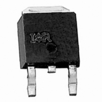
IC SWITCH IPS 1CH LOW SIDE DPAK
Manufacturer
International Rectifier
Type
Low Sider
Datasheet
1.IPS1021RTRRPBF.pdf
(14 pages)
Specifications of IPS1021RPBF
Input Type
Non-Inverting
Number Of Outputs
1
On-state Resistance
20 mOhm
Current - Output / Channel
4.3A
Current - Peak Output
45A
Voltage - Supply
4.5 V ~ 5.5 V
Operating Temperature
-40°C ~ 150°C
Mounting Type
Surface Mount
Package / Case
DPak, TO-252 (2 leads+tab), SC-63
Switch Type
Low Side
Power Switch Family
IPS1021
Input Voltage
4.5 to 5.5V
Power Switch On Resistance
20mOhm
Output Current
4.3A
Mounting
Surface Mount
Package Type
DPAK
Operating Temperature (min)
-40C
Operating Temperature (max)
150C
Operating Temperature Classification
Automotive
Pin Count
2 +Tab
Power Dissipation
2.5W
Power Load Switch Type
Single Low Side
On State Resistance
0.02ohm
Thermal Protection
Yes
Power Dissipation Pd
2.5W
No. Of Outputs
1
Internal Switch
Yes
Rohs Compliant
Yes
Lead Free Status / RoHS Status
Lead free / RoHS Compliant


Static Electrical Characteristics
Tj=25°C, Vcc=14V (unless otherwise specified)
Switching Electrical Characteristics
Vcc=14V, Resistive load=1.5Ω, Rinput=0Ω, Vin=5V, Tj=25°C
Protection Characteristics
Diagnostic
(2) Guaranteed by design
www.irf.com
Symbol
Rds(on)
Idss1
Idss2
V clamp1
V clamp2
Vin clamp
Vth
Symbol
Tdon
Tr
Tdoff
Tf
Eon + Eoff
Symbol
Tsd
Isd
OV
Vreset
Treset
Symbol
Iin, on
Iin, off
Over temperature threshold
Over current threshold
Over voltage protection ( not active when
the device is ON )
IN protection reset threshold
Time to reset protection
Parameter
ON state resistance Tj=25°C
ON state resistance Tj=150°C (2)
Drain to source leakage current
Drain to source leakage current
Drain to source clamp voltage 1
Drain to source clamp voltage 2
IN to source pin clamp voltage
Input threshold voltage
Parameter
ON state IN positive current
OFF state IN positive current
(after protection latched)
Parameter
Turn-on delay time to 20%
Rise time 20% to 80%
Turn-off delay time to 80%
Fall time 80% to 20%
Turn on and off energy
Parameter
Min.
150(2)
Min.
Min.
Min.
15(2)
150
5.5
10
10
40
15
36
⎯
32
34
15
⎯
⎯
⎯
⎯
⎯
⎯
⎯
Typ.
Typ.
Typ.
Typ.
150
165
1.7
230
0.1
0.2
6.5
1.7
30
30
30
45
37
50
20
38
39
40
32
2
Max.
Max.
Max.
Max.
100
400
200
350
7.5
60
60
58
25
48
10
20
42
⎯
⎯
⎯
⎯
70
⎯
⎯
IPS1021(
Units
Units
Units
Units
mΩ
mJ
µA
µs
µA
°C
µs
V
A
V
V
Test Conditions
See figure 2
Vin=5V, Ids=8A
Vcc=28V, Tj=25°C
Id=20mA
Id=2A
Iin=1mA
Id=10mA
Vin=5V
Vin=5V
Test Conditions
Vcc=14V, Tj=25°C
Test Conditions
Test Conditions
See figure 1
See figure 1
Vin=0V
S
)(
R
)PbF
3
Related parts for IPS1021RPBF
Image
Part Number
Description
Manufacturer
Datasheet
Request
R

Part Number:
Description:
low-side intelligent power switches (IPS)
Manufacturer:
International Rectifier Corp.
Datasheet:

Part Number:
Description:
CONN RCPT .100" 6POS DUAL PCB
Manufacturer:
Samtec Inc
Datasheet:

Part Number:
Description:
CONN RCPT .100" 20POS DUAL PCB
Manufacturer:
Samtec Inc
Datasheet:

Part Number:
Description:
CONN RCPT .100" 10POS DUAL PCB
Manufacturer:
Samtec Inc
Datasheet:
Part Number:
Description:
CONN RCPT .100" 10POS DL PCB SMD
Manufacturer:
Samtec Inc
Datasheet:

Part Number:
Description:
CONN RCPT .100" 10POS DL PCB R/A
Manufacturer:
Samtec Inc
Datasheet:

Part Number:
Description:
CONN RCPT .100" 20POS DL PCB R/A
Manufacturer:
Samtec Inc
Datasheet:

Part Number:
Description:
CONN RCPT .100" 30POS DUAL PCB
Manufacturer:
Samtec Inc
Datasheet:
Part Number:
Description:
CONN RCPT .100" 30POS DL PCB SMD
Manufacturer:
Samtec Inc
Datasheet:

Part Number:
Description:
CONN RCPT .100" 30POS DL PCB R/A
Manufacturer:
Samtec Inc
Datasheet:
Part Number:
Description:
SCHOTTKY RECTIFIER
Manufacturer:
International Rectifier Corp.
Datasheet:
Part Number:
Description:
SCHOTTKY RECTIFIER
Manufacturer:
International Rectifier Corp.
Datasheet:
Part Number:
Description:
SCHOTTKY RECTIFIER
Manufacturer:
International Rectifier Corp.
Datasheet:
Part Number:
Description:
SCHOTTKY RECTIFIER
Manufacturer:
International Rectifier Corp.
Datasheet:
Part Number:
Description:
SCHOTTKY RECTIFIER
Manufacturer:
International Rectifier Corp.
Datasheet: