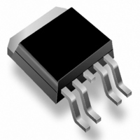
IPS7091SPBF International Rectifier, IPS7091SPBF Datasheet - Page 2

IPS7091SPBF
Manufacturer Part Number
IPS7091SPBF
Description
IC SWITCH IPS 1CH HI SIDE D2PAK-
Manufacturer
International Rectifier
Type
High Sider
Specifications of IPS7091SPBF
Input Type
Non-Inverting
Number Of Outputs
1
On-state Resistance
80 mOhm
Current - Output / Channel
1.5A
Current - Peak Output
5A
Voltage - Supply
6 V ~ 35 V
Operating Temperature
-40°C ~ 150°C
Mounting Type
Surface Mount
Package / Case
D²Pak, TO-263 (4 leads + tab)
Switch Type
High Side
Power Switch Family
IPS7091
Input Voltage
-0.3 to 5.5V
Power Switch On Resistance
90mOhm
Output Current
1.5A
Mounting
Surface Mount
Supply Current
2.5mA
Package Type
D2PAK
Operating Temperature (min)
-40C
Operating Temperature (max)
150C
Operating Temperature Classification
Automotive
Pin Count
4 +Tab
Power Dissipation
1.25W
Current, Drain
1.5 A
Current, Input
80 μA
Current, Leakage, Offset
10 μA
Current, Supply
3.5 A
Polarization
N-Channel
Resistance, Drain To Source On
120 Milliohms
Temperature, Operating, Maximum
+150 °C
Temperature, Operating, Minimum
–40 °C
Thermal Resistance, Junction To Ambient
100 °C/W
Time, Turn-off Delay
45 μs
Time, Turn-on Delay
35 μs
Voltage, Input
5.5 V
Voltage, Input, High Level
5.5 V
Voltage, Input, Low Level
0.9 V
Voltage, Supply
65 V
Power Load Switch Type
High Side
Current Limit
5A
On State Resistance
0.08ohm
Thermal Protection
ESD
Power Dissipation Pd
1.25W
No. Of Outputs
1
Internal Switch
No
Rohs Compliant
Yes
Lead Free Status / RoHS Status
Lead free / RoHS Compliant
Absolute Maximum Ratings
Absolute maximum ratings indicate sustained limits beyond which damage to the device may occur. All voltage parameters
are referenced to Ground lead. (Tambient=25°C unless otherwise specified).
Thermal Characteristics
Recommended Operating Conditions
These values are given for a quick design. For operation outside these conditions, please consult the application notes.
www.irf.com
Symbol
Rth1
Rth1
Rth1
Rth2
Rth3
Symbol
VIH
VIL
Iout
Rin
Rdgs
Rol
Symbol
Vout
Voffset
Vin
Vcc max.
Vcc cont.
Iin max.
Idg max.
Vdg
Pd
Isd cont.
ESD1
ESD2
Tj max.
Parameter
Maximum input voltage
Maximum IN current
Maximum output voltage
Maximum logic ground to load ground offset
Maximum Vcc voltage
Maximum continuous Vcc voltage
Maximum diagnostic output current
Maximum diagnostic output voltage
Maximum power dissipation (internally limited by thermal protection)
Maximum continuous diode current (Rth=100°C/W)
Electrostatic discharge voltage (Human body) 100pF, 1500Ω
Electrostatic discharge voltage (Machine Model) C=200pF,R=0Ω,L=10µH
Max. storage & operating temperature junction temperature
Parameter
Parameter
Low level input voltage
Recommended resistor in series with IN pin
Recommended resistor in series with DG pin
Recommended pull-up resistor for open load detection
Thermal resistance junction to ambient SO8 std. footprint
Thermal resistance junction to ambient TO220 free air
Thermal resistance junction to ambient D2Pak std. footprint
Thermal resistance junction to ambient D2Pak 1” sqrt. footprint
Thermal resistance junction to case D2pak/TO220
High level input voltage
Continuous drain current, Tamb=85°C, Tj=125°C, Vin=5V, Rth=100°C/W
Rth=100°C/W
IPS7091(G)(S)PbF
Vcc-65 Vcc+0.3
Vcc-65 Vcc+0.3
Typ.
Min.
Min.
-0.3
-0.3
-0.3
100
-40
60
60
40
10
10
⎯
⎯
-1
-1
⎯
⎯
⎯
⎯
⎯
4
4
5
Max.
Max.
Max.
+150
1.25
100
5.5
5.5
1.8
0.5
5.5
0.9
1.5
20
20
65
35
10
10
⎯
⎯
⎯
⎯
⎯
4
Units
Units
°C/W
Units
2
mA
kV
°C
k
W
V
V
A
A
Ω


