IPS7091SPBF International Rectifier, IPS7091SPBF Datasheet - Page 4
IPS7091SPBF
Manufacturer Part Number
IPS7091SPBF
Description
IC SWITCH IPS 1CH HI SIDE D2PAK-
Manufacturer
International Rectifier
Type
High Sider
Specifications of IPS7091SPBF
Input Type
Non-Inverting
Number Of Outputs
1
On-state Resistance
80 mOhm
Current - Output / Channel
1.5A
Current - Peak Output
5A
Voltage - Supply
6 V ~ 35 V
Operating Temperature
-40°C ~ 150°C
Mounting Type
Surface Mount
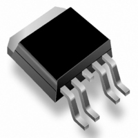
Package / Case
D²Pak, TO-263 (4 leads + tab)
Switch Type
High Side
Power Switch Family
IPS7091
Input Voltage
-0.3 to 5.5V
Power Switch On Resistance
90mOhm
Output Current
1.5A
Mounting
Surface Mount
Supply Current
2.5mA
Package Type
D2PAK
Operating Temperature (min)
-40C
Operating Temperature (max)
150C
Operating Temperature Classification
Automotive
Pin Count
4 +Tab
Power Dissipation
1.25W
Current, Drain
1.5 A
Current, Input
80 μA
Current, Leakage, Offset
10 μA
Current, Supply
3.5 A
Polarization
N-Channel
Resistance, Drain To Source On
120 Milliohms
Temperature, Operating, Maximum
+150 °C
Temperature, Operating, Minimum
–40 °C
Thermal Resistance, Junction To Ambient
100 °C/W
Time, Turn-off Delay
45 μs
Time, Turn-on Delay
35 μs
Voltage, Input
5.5 V
Voltage, Input, High Level
5.5 V
Voltage, Input, Low Level
0.9 V
Voltage, Supply
65 V
Power Load Switch Type
High Side
Current Limit
5A
On State Resistance
0.08ohm
Thermal Protection
ESD
Power Dissipation Pd
1.25W
No. Of Outputs
1
Internal Switch
No
Rohs Compliant
Yes
Lead Free Status / RoHS Status
Lead free / RoHS Compliant


Protection Characteristics
(1
(2
T
(3
Lead Assignments
www.irf.com
)
)
)
Symbol
Ilim
Tsd+
Tsd-
Vsc
Vopen load
Operatin
Normal
Normal
Open Load
Open Load
Short circuit to
Short circuit to
Over-temperature
Over-temperature
ruth
Guarantee
Reference
With a p
Tabl
8 7 6 5
1 2 3 4
SO
ull-up
g C
d b
to
(3)
8
Internal current limit
Over temperature high threshold
Over temperature low threshold
Short-circuit detection voltage
Open load detection threshold
Vcc
onditions
y design
e
Gnd
Gnd
Parameter
resistor connected between the outpu
1- Gnd
2- In
3- DG
4- Out
5-6-7-8 Vcc
IN
H
H
H
H
L
L
L
L
L (l
L (cycling)
OUT
imiting)
(2)
H
H
H
L
L
L
t and V
DG pin
1 2 3 4 5
TO220
3- Vcc
150
H
H
H
Min.
L
L
L
L
L
cc.
⎯
2
2
2
(1)
Typ.
165
158
5
3
3
Max.
1- G
2- In
3- V
4- D
5- O
⎯
⎯
8
4
4
cc
g
nd
ut
IPS7091(G)(S)PbF
Units
°C
A
V
Test Conditions
Vout=0V
See Fig. 2
1 2 3 4 5
D²Pak
3- Vcc
4
Related parts for IPS7091SPBF
Image
Part Number
Description
Manufacturer
Datasheet
Request
R

Part Number:
Description:
Intelligent Power HIGH SIDE Switch
Manufacturer:
International Rectifier Corp.
Datasheet:
Part Number:
Description:
SCHOTTKY RECTIFIER
Manufacturer:
International Rectifier Corp.
Datasheet:
Part Number:
Description:
SCHOTTKY RECTIFIER
Manufacturer:
International Rectifier Corp.
Datasheet:
Part Number:
Description:
SCHOTTKY RECTIFIER
Manufacturer:
International Rectifier Corp.
Datasheet:
Part Number:
Description:
SCHOTTKY RECTIFIER
Manufacturer:
International Rectifier Corp.
Datasheet:
Part Number:
Description:
SCHOTTKY RECTIFIER
Manufacturer:
International Rectifier Corp.
Datasheet:
Part Number:
Description:
SCHOTTKY RECTIFIER
Manufacturer:
International Rectifier Corp.
Datasheet:
Part Number:
Description:
SCHOTTKY RECTIFIER
Manufacturer:
International Rectifier Corp.
Datasheet:
Part Number:
Description:
SCHOTTKY RECTIFIER
Manufacturer:
International Rectifier Corp.
Datasheet:
Part Number:
Description:
SCHOTTKY RECTIFIER
Manufacturer:
International Rectifier Corp.
Datasheet:
Part Number:
Description:
SCHOTTKY RECTIFIER
Manufacturer:
International Rectifier Corp.
Datasheet:
Part Number:
Description:
SCHOTTKY RECTIFIER
Manufacturer:
International Rectifier Corp.
Datasheet:
Part Number:
Description:
SCHOTTKY RECTIFIER
Manufacturer:
International Rectifier Corp.
Datasheet:
Part Number:
Description:
SCHOTTKY RECTIFIER
Manufacturer:
International Rectifier Corp.
Datasheet:
Part Number:
Description:
SCHOTTKY RECTIFIER
Manufacturer:
International Rectifier Corp.
Datasheet: